DK-DEV-2AGX125N Altera, DK-DEV-2AGX125N Datasheet - Page 88
DK-DEV-2AGX125N
Manufacturer Part Number
DK-DEV-2AGX125N
Description
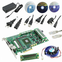
KIT DEV ARRIA II GX FPGA 2AGX125
Manufacturer
Altera
Series
Arria II GXr
Type
FPGAr
Datasheets
1.EP2AGX45CU17C6N.pdf
(96 pages)
2.DK-DEV-2AGX125N.pdf
(48 pages)
3.DK-DEV-2AGX125N.pdf
(64 pages)
Specifications of DK-DEV-2AGX125N
Contents
Board, Cables, CD, DVD, Power Supply
Silicon Manufacturer
Altera
Core Architecture
FPGA
Core Sub-architecture
Arria
Silicon Core Number
EP2
Silicon Family Name
Arria II GX
Rohs Compliant
Yes
For Use With/related Products
EP2AGX125EF35
Lead Free Status / RoHS Status
Lead free / RoHS Compliant
Other names
544-2600
Available stocks
Company
Part Number
Manufacturer
Quantity
Price
Company:

Part Number:
DK-DEV-2AGX125N
Manufacturer:
Altera
Quantity:
135


1–80
Table 1–67. Glossary (Part 3 of 4)
Arria II Device Handbook Volume 3: Device Datasheet and Addendum
Letter
S
T
SW (sampling
window)
Single-ended
Voltage
Referenced I/O
Standard
t
TCCS
(channel-to-
channel-
skew)
t
t
t
t
t
t
C
DUTY
FALL
INCCJ
OUTPJ_IO
OUTPJ_DC
RISE
Subject
The period of time during which the data must be valid in order to capture it correctly. The setup
and hold times determine the ideal strobe position within the sampling window:
Timing Diagram
The JEDEC standard for SSTL and HSTL I/O standards define both the AC and DC input signal
values. The AC values indicate the voltage levels at which the receiver must meet its timing
specifications. The DC values indicate the voltage levels at which the final logic state of the
receiver is unambiguously defined. After the receiver input has crossed the AC value, the receiver
changes to the new logic state.
The new logic state is then maintained as long as the input stays beyond the AC threshold. This
approach is intended to provide predictable receiver timing in the presence of input waveform
ringing:
Single-Ended Voltage Referenced I/O Standard
High-speed receiver and transmitter input and output clock period.
The timing difference between the fastest and slowest output edges, including t
clock skew, across channels driven by the same PLL. The clock is included in the TCCS
measurement (refer to the Timing Diagram figure under S in this table).
High-speed I/O block: Duty cycle on the high-speed transmitter output clock.
Timing Unit Interval (TUI)
The timing budget allowed for skew, propagation delays, and data sampling window.
(TUI = 1/(Receiver Input Clock Frequency Multiplication Factor) = t
Signal high-to-low transition time (80-20%)
Cycle-to-cycle jitter tolerance on the PLL clock input.
Period jitter on the general purpose I/O driven by a PLL.
Period jitter on the dedicated clock output driven by a PLL.
Signal low-to-high transition time (20-80%).
V
V
OH
OL
0.5 x TCCS
RSKM
Definitions
Sampling Window
V
Bit Time
REF
(SW)
Chapter 1: Device Datasheet for Arria II Devices
RSKM
C
V
/w)
December 2010 Altera Corporation
V
IH(DC)
IL(DC)
0.5 x TCCS
V
V
IH ( AC )
IL(AC )
CO
V
CCIO
V
variation and
SS
Glossary
Related parts for DK-DEV-2AGX125N
Image
Part Number
Description
Manufacturer
Datasheet
Request
R

Part Number:
Description:
KIT DEV CYCLONE III LS EP3CLS200
Manufacturer:
Altera
Datasheet:

Part Number:
Description:
KIT DEV STRATIX IV FPGA 4SE530
Manufacturer:
Altera
Datasheet:

Part Number:
Description:
KIT DEV FPGA 2AGX260 W/6.375G TX
Manufacturer:
Altera
Datasheet:

Part Number:
Description:
KIT DEV MAX V 5M570Z
Manufacturer:
Altera
Datasheet:

Part Number:
Description:
KIT DEV STRATIX V FPGA 5SGXEA7
Manufacturer:
Altera
Datasheet:

Part Number:
Description:
KIT DEVELOPMENT STRATIX III
Manufacturer:
Altera
Datasheet:

Part Number:
Description:
KIT DEVELOPMENT STRATIX IV
Manufacturer:
Altera
Datasheet:

Part Number:
Description:
KIT DEV ARRIA GX 1AGX60N
Manufacturer:
Altera
Datasheet:
Part Number:
Description:
KIT STARTER CYCLONE IV GX
Manufacturer:
Altera
Datasheet:
Part Number:
Description:
KIT DEVELOPMENT STRATIX IV
Manufacturer:
Altera
Datasheet:

Part Number:
Description:
CPLD, EP610 Family, ECMOS Process, 300 Gates, 16 Macro Cells, 16 Reg., 16 User I/Os, 5V Supply, 35 Speed Grade, 24DIP
Manufacturer:
Altera Corporation
Datasheet:
Part Number:
Description:
CPLD, EP610 Family, ECMOS Process, 300 Gates, 16 Macro Cells, 16 Reg., 16 User I/Os, 5V Supply, 15 Speed Grade, 24DIP
Manufacturer:
Altera Corporation
Datasheet: