DK-DEV-3CLS200N Altera, DK-DEV-3CLS200N Datasheet - Page 14
DK-DEV-3CLS200N
Manufacturer Part Number
DK-DEV-3CLS200N
Description
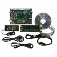
KIT DEV CYCLONE III LS EP3CLS200
Manufacturer
Altera
Series
Cyclone® IIIr
Type
FPGAr
Datasheets
1.EP3C5F256C8N.pdf
(34 pages)
2.EP3C5F256C8N.pdf
(14 pages)
3.DK-START-3C25N.pdf
(74 pages)
4.DK-DEV-3CLS200N.pdf
(42 pages)
Specifications of DK-DEV-3CLS200N
Contents
Board
Silicon Manufacturer
Altera
Core Architecture
FPGA
Core Sub-architecture
Cyclone
Silicon Core Number
EP3C
Silicon Family Name
Cyclone III LS
Rohs Compliant
Yes
For Use With/related Products
EP3CLS200
Lead Free Status / RoHS Status
Lead free / RoHS Compliant
Other names
544-2601


4–2
Factory Default Switch Settings
Cyclone III LS FPGA Development Kit User Guide
This section shows the factory switch settings for the Cyclone III LS FPGA
development board.
position of each switch.
Figure 4–1. Switch Locations and Default Settings on the FPGA Development Board
To restore the switches to their factory default settings, perform the following steps:
1. Set DIP switch bank (S7) to match
Table 4–1. S7 Dip Switch Settings
2. Set DIP switch bank (SW2) to match
Table 4–2. SW2 Dip Switch Settings
1
2
3
4
1
2
3
4
5
6
7
8
Switch
Switch
J18
LCD SEL
Figure 4–1
On
On
On
On
On
On
On
On
Off
On
Off
Off
(not installed)
Position
Position
shows the switch bank locations and the default
S7
Table 4–1
E P3CLS200F780
DIP Switch
Table 4–2
User
4 3 2 1
ON
OFF = 1
ON = 0
and
and
Figure
Figure
J11
J12
JTAG Control Jumpers
Chapter 4: Development Board Setup
4–1.
© October 2009 Altera Corporation
ON = 0
OFF = 1
4–1.
Factory Default Switch Settings
(installed)
(not installed)
(not installed)
(not installed)
Board Settings
DIP Switch
8
7
SW2
6
OPEN
5
4
3
2
1
Related parts for DK-DEV-3CLS200N
Image
Part Number
Description
Manufacturer
Datasheet
Request
R

Part Number:
Description:
KIT DEV ARRIA II GX FPGA 2AGX125
Manufacturer:
Altera
Datasheet:

Part Number:
Description:
KIT DEV STRATIX IV FPGA 4SE530
Manufacturer:
Altera
Datasheet:

Part Number:
Description:
KIT DEV FPGA 2AGX260 W/6.375G TX
Manufacturer:
Altera
Datasheet:

Part Number:
Description:
KIT DEV MAX V 5M570Z
Manufacturer:
Altera
Datasheet:

Part Number:
Description:
KIT DEV STRATIX V FPGA 5SGXEA7
Manufacturer:
Altera
Datasheet:

Part Number:
Description:
KIT DEVELOPMENT STRATIX III
Manufacturer:
Altera
Datasheet:

Part Number:
Description:
KIT DEVELOPMENT STRATIX IV
Manufacturer:
Altera
Datasheet:

Part Number:
Description:
KIT DEV ARRIA GX 1AGX60N
Manufacturer:
Altera
Datasheet:
Part Number:
Description:
KIT STARTER CYCLONE IV GX
Manufacturer:
Altera
Datasheet:
Part Number:
Description:
KIT DEVELOPMENT STRATIX IV
Manufacturer:
Altera
Datasheet:

Part Number:
Description:
CPLD, EP610 Family, ECMOS Process, 300 Gates, 16 Macro Cells, 16 Reg., 16 User I/Os, 5V Supply, 35 Speed Grade, 24DIP
Manufacturer:
Altera Corporation
Datasheet:
Part Number:
Description:
CPLD, EP610 Family, ECMOS Process, 300 Gates, 16 Macro Cells, 16 Reg., 16 User I/Os, 5V Supply, 15 Speed Grade, 24DIP
Manufacturer:
Altera Corporation
Datasheet: