TOOLSTICK560DC Silicon Laboratories Inc, TOOLSTICK560DC Datasheet - Page 11
TOOLSTICK560DC
Manufacturer Part Number
TOOLSTICK560DC
Description
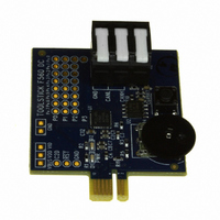
DAUGHTER CARD TOOLSTICK F560
Manufacturer
Silicon Laboratories Inc
Series
ToolStickr
Type
MCUr
Specifications of TOOLSTICK560DC
Contents
Daughter Card
Processor To Be Evaluated
C8051F55x, C8051F56x, C8051F57x
Interface Type
USB
Operating Supply Voltage
2.7 V to 3.6 V
Lead Free Status / RoHS Status
Lead free / RoHS Compliant
For Use With/related Products
C8051F55x, C8051F56x, C8051F57x
For Use With
336-1345 - TOOLSTICK BASE ADAPTER336-1182 - ADAPTER USB DEBUG FOR C8051FXXX
Lead Free Status / Rohs Status
Lead free / RoHS Compliant
Other names
336-1719


C8051F55x/56x/57x
List of Tables
Table 2.1. Product Selection Guide ......................................................................... 21
Table 3.1. Pin Definitions for the C8051F55x/56x/57x ............................................ 22
Table 4.1. QFN-40 Package Dimensions ................................................................ 28
Table 4.2. QFN-40 Landing Diagram Dimensions ................................................... 29
Table 4.3. QFP-32 Package Dimensions ................................................................ 30
Table 4.4. QFP-32 Landing Diagram Dimensions ................................................... 31
Table 4.5. QFN-32 Package Dimensions ................................................................ 32
Table 4.6. QFN-32 Landing Diagram Dimensions ................................................... 33
Table 4.7. QFN-24 Package Dimensions ................................................................ 34
Table 4.8. QFN-24 Landing Diagram Dimensions ................................................... 35
Table 5.1. Absolute Maximum Ratings .................................................................... 36
Table 5.2. Global Electrical Characteristics ............................................................. 37
Table 5.3. Port I/O DC Electrical Characteristics ..................................................... 40
Table 5.4. Reset Electrical Characteristics .............................................................. 41
Table 5.5. Flash Electrical Characteristics .............................................................. 41
Table 5.6. Internal High-Frequency Oscillator Electrical Characteristics ................. 42
Table 5.7. Clock Multiplier Electrical Specifications ................................................ 43
Table 5.8. Voltage Regulator Electrical Characteristics .......................................... 43
Table 5.9. ADC0 Electrical Characteristics .............................................................. 44
Table 5.10. Temperature Sensor Electrical Characteristics .................................... 45
Table 5.11. Voltage Reference Electrical Characteristics ....................................... 45
Table 5.12. Comparator 0 and Comparator 1 Electrical Characteristics ................. 46
Table 10.1. CIP-51 Instruction Set Summary .......................................................... 84
Table 12.1. Special Function Register (SFR) Memory Map for Pages
0x00 and 0x0F .................................................................................... 106
Table 12.2. Special Function Register (SFR) Memory Map for Page 0x0C .......... 107
Table 12.3. Special Function Registers ................................................................. 108
Table 13.1. Interrupt Summary .............................................................................. 114
Table 14.1. Flash Security Summary .................................................................... 127
Table 17.1. EMIF Pinout (C8051F568-9 and ‘F570-5) .......................................... 144
Table 17.2. AC Parameters for External Memory Interface ................................... 154
Table 19.1. Port I/O Assignment for Analog Functions ......................................... 169
Table 19.2. Port I/O Assignment for Digital Functions ........................................... 169
Table 19.3. Port I/O Assignment for External Digital Event Capture Functions .... 170
Table 20.1. Baud Rate Calculation Variable Ranges ............................................ 192
Table 20.2. Manual Baud Rate Parameters Examples ......................................... 194
Table 20.3. Autobaud Parameters Examples ........................................................ 195
Table 20.4. LIN Registers* (Indirectly Addressable) .............................................. 200
Table 21.1. Background System Information ........................................................ 210
Table 21.2. Standard CAN Registers and Reset Values ....................................... 213
Table 22.1. SMBus Clock Source Selection .......................................................... 220
Table 22.2. Minimum SDA Setup and Hold Times ................................................ 221
Rev. 1.1
11
Related parts for TOOLSTICK560DC
Image
Part Number
Description
Manufacturer
Datasheet
Request
R

Part Number:
Description:
KIT TOOL EVAL SYS IN A USB STICK
Manufacturer:
Silicon Laboratories Inc
Datasheet:

Part Number:
Description:
TOOLSTICK DEBUG ADAPTER
Manufacturer:
Silicon Laboratories Inc
Datasheet:

Part Number:
Description:
TOOLSTICK BASE ADAPTER
Manufacturer:
Silicon Laboratories Inc
Datasheet:

Part Number:
Description:
TOOLSTICK DAUGHTER CARD
Manufacturer:
Silicon Laboratories Inc
Datasheet:

Part Number:
Description:
TOOLSTICK DAUGHTER CARD
Manufacturer:
Silicon Laboratories Inc
Datasheet:

Part Number:
Description:
TOOLSTICK DAUGHTER CARD
Manufacturer:
Silicon Laboratories Inc
Datasheet:

Part Number:
Description:
TOOLSTICK PROGRAMMING ADAPTER
Manufacturer:
Silicon Laboratories Inc
Datasheet:

Part Number:
Description:
TOOLSTICK DAUGHTER CARD
Manufacturer:
Silicon Laboratories Inc
Datasheet:

Part Number:
Description:
KIT STARTER TOOLSTICK
Manufacturer:
Silicon Laboratories Inc
Datasheet:

Part Number:
Description:
KIT UNIVERSITY TOOLSTICK STARTER
Manufacturer:
Silicon Laboratories Inc
Datasheet:

Part Number:
Description:
DAUGHTER CARD TOOLSTICK F330
Manufacturer:
Silicon Laboratories Inc
Datasheet:

Part Number:
Description:
CARD DAUGHTER UNIVRSTY TOOLSTICK
Manufacturer:
Silicon Laboratories Inc
Datasheet:

Part Number:
Description:
DAUGHTER CARD TOOLSTICK F582
Manufacturer:
Silicon Laboratories Inc
Datasheet:

Part Number:
Description:
DAUGHTER CARD TOOLSTICK F500
Manufacturer:
Silicon Laboratories Inc
Datasheet:

Part Number:
Description:
DAUGHTER CARD TOOLSTICK F540
Manufacturer:
Silicon Laboratories Inc
Datasheet: