TOOLSTICK560DC Silicon Laboratories Inc, TOOLSTICK560DC Datasheet - Page 167
TOOLSTICK560DC
Manufacturer Part Number
TOOLSTICK560DC
Description
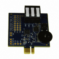
DAUGHTER CARD TOOLSTICK F560
Manufacturer
Silicon Laboratories Inc
Series
ToolStickr
Type
MCUr
Specifications of TOOLSTICK560DC
Contents
Daughter Card
Processor To Be Evaluated
C8051F55x, C8051F56x, C8051F57x
Interface Type
USB
Operating Supply Voltage
2.7 V to 3.6 V
Lead Free Status / RoHS Status
Lead free / RoHS Compliant
For Use With/related Products
C8051F55x, C8051F56x, C8051F57x
For Use With
336-1345 - TOOLSTICK BASE ADAPTER336-1182 - ADAPTER USB DEBUG FOR C8051FXXX
Lead Free Status / Rohs Status
Lead free / RoHS Compliant
Other names
336-1719


19. Port Input/Output
Digital and analog resources are available through 33 (C8051F568-9 and ‘F570-5), 25 (C8051F550-7) or
18 (C8051F550-7) I/O pins. Port pins P0.0-P4.0 on the C8051F568-9 and ‘F570-5, port pins P0.0-P3.0 on
theC8051F560-7, and port pins P0.0-P2.1 on the C8051F550-7 can be defined as general-purpose I/O
(GPIO), assigned to one of the internal digital resources, or assigned to an analog function as shown in
Figure 19.3. Port pin P4.0 on the C8051F568-9 and ‘F570-5 can be used as GPIO and is shared with the
C2 Interface Data signal (C2D). Similarly, port pin P3.0 is shared with C2D on the C8051F560-7 and port
pin P2.1 on the C8051F550-7. The designer has complete control over which functions are assigned, lim-
ited only by the number of physical I/O pins. This resource assignment flexibility is achieved through the
use of a Priority Crossbar Decoder. Note that the state of a Port I/O pin can always be read in the corre-
sponding Port latch, regardless of the Crossbar settings.
The Crossbar assigns the selected internal digital resources to the I/O pins based on the Priority Decoder
(Figure 19.3 and Figure 19.4). The registers XBR0, XBR1, XBR2 are defined in SFR Definition 19.1 and
SFR Definition 19.2 and are used to select internal digital functions.
The Port I/O cells are configured as either push-pull or open-drain in the Port Output Mode registers
(PnMDOUT, where n = 0,1). Complete Electrical Specifications for Port I/O are given in Table 5.3 on
page 40.
Highest
Lowest
Priority
Priority
Latches
Port
/SYSCLK
SMBus0
UART0
T0, T1,
/INT0,
CAN0
PCA0
/INT1
SPI0
LIN0
CP0
CP1
P0
P1
P2
P3
P4
(Px.0-Px.7)
33
Figure 19.1. Port I/O Functional Block Diagram
2
2
4
2
2
2
7
4
2
XBR2, PnSKIP
XBR0, XBR1,
Crossbar
Decoder
Priority
Rev. 1.1
Digital
8
8
8
8
8
C8051F55x/56x/57x
PnDMIN Registers
PnMDOUT,
Cells
Cells
Cells
Cells
Cell
I/O
I/O
I/O
I/O
I/O
P0
P1
P2
P3
P4
PnMATCH
Registers
PnMASK
External
Pins
P0.0
P0.7
P1.0
P1.7
P2.0
P2.7
P3.0
P3.7
P4.0
Highest
Priority
Lowest
Priority
167
Related parts for TOOLSTICK560DC
Image
Part Number
Description
Manufacturer
Datasheet
Request
R

Part Number:
Description:
KIT TOOL EVAL SYS IN A USB STICK
Manufacturer:
Silicon Laboratories Inc
Datasheet:

Part Number:
Description:
TOOLSTICK DEBUG ADAPTER
Manufacturer:
Silicon Laboratories Inc
Datasheet:

Part Number:
Description:
TOOLSTICK BASE ADAPTER
Manufacturer:
Silicon Laboratories Inc
Datasheet:

Part Number:
Description:
TOOLSTICK DAUGHTER CARD
Manufacturer:
Silicon Laboratories Inc
Datasheet:

Part Number:
Description:
TOOLSTICK DAUGHTER CARD
Manufacturer:
Silicon Laboratories Inc
Datasheet:

Part Number:
Description:
TOOLSTICK DAUGHTER CARD
Manufacturer:
Silicon Laboratories Inc
Datasheet:

Part Number:
Description:
TOOLSTICK PROGRAMMING ADAPTER
Manufacturer:
Silicon Laboratories Inc
Datasheet:

Part Number:
Description:
TOOLSTICK DAUGHTER CARD
Manufacturer:
Silicon Laboratories Inc
Datasheet:

Part Number:
Description:
KIT STARTER TOOLSTICK
Manufacturer:
Silicon Laboratories Inc
Datasheet:

Part Number:
Description:
KIT UNIVERSITY TOOLSTICK STARTER
Manufacturer:
Silicon Laboratories Inc
Datasheet:

Part Number:
Description:
DAUGHTER CARD TOOLSTICK F330
Manufacturer:
Silicon Laboratories Inc
Datasheet:

Part Number:
Description:
CARD DAUGHTER UNIVRSTY TOOLSTICK
Manufacturer:
Silicon Laboratories Inc
Datasheet:

Part Number:
Description:
DAUGHTER CARD TOOLSTICK F582
Manufacturer:
Silicon Laboratories Inc
Datasheet:

Part Number:
Description:
DAUGHTER CARD TOOLSTICK F500
Manufacturer:
Silicon Laboratories Inc
Datasheet:

Part Number:
Description:
DAUGHTER CARD TOOLSTICK F540
Manufacturer:
Silicon Laboratories Inc
Datasheet: