TOOLSTICK560DC Silicon Laboratories Inc, TOOLSTICK560DC Datasheet - Page 4
TOOLSTICK560DC
Manufacturer Part Number
TOOLSTICK560DC
Description
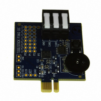
DAUGHTER CARD TOOLSTICK F560
Manufacturer
Silicon Laboratories Inc
Series
ToolStickr
Type
MCUr
Specifications of TOOLSTICK560DC
Contents
Daughter Card
Processor To Be Evaluated
C8051F55x, C8051F56x, C8051F57x
Interface Type
USB
Operating Supply Voltage
2.7 V to 3.6 V
Lead Free Status / RoHS Status
Lead free / RoHS Compliant
For Use With/related Products
C8051F55x, C8051F56x, C8051F57x
For Use With
336-1345 - TOOLSTICK BASE ADAPTER336-1182 - ADAPTER USB DEBUG FOR C8051FXXX
Lead Free Status / Rohs Status
Lead free / RoHS Compliant
Other names
336-1719


C8051F55x/56x/57x
13. Interrupts .............................................................................................................. 112
14. Flash Memory....................................................................................................... 124
15. Power Management Modes................................................................................. 133
16. Reset Sources ...................................................................................................... 136
17. External Data Memory Interface and On-Chip XRAM ....................................... 142
4
12.2. Interrupts and SFR Paging .............................................................................. 95
12.3. SFR Page Stack Example ............................................................................... 97
13.1. MCU Interrupt Sources and Vectors.............................................................. 112
13.2. Interrupt Register Descriptions ...................................................................... 115
13.3. External Interrupts INT0 and INT1................................................................. 122
14.1. Programming The Flash Memory .................................................................. 124
14.2. Non-volatile Data Storage ............................................................................. 126
14.3. Security Options ............................................................................................ 126
14.4. Flash Write and Erase Guidelines ................................................................. 128
15.1. Idle Mode....................................................................................................... 133
15.2. Stop Mode ..................................................................................................... 134
15.3. Suspend Mode .............................................................................................. 134
16.1. Power-On Reset ............................................................................................ 137
16.2. Power-Fail Reset/VDD Monitor ..................................................................... 137
16.3. External Reset ............................................................................................... 139
16.4. Missing Clock Detector Reset ....................................................................... 139
16.5. Comparator0 Reset ....................................................................................... 140
16.6. PCA Watchdog Timer Reset ......................................................................... 140
16.7. Flash Error Reset .......................................................................................... 140
16.8. Software Reset .............................................................................................. 140
17.1. Accessing XRAM........................................................................................... 142
17.2. Configuring the External Memory Interface ................................................... 143
17.3. Port Configuration.......................................................................................... 143
17.4. Multiplexed Mode .......................................................................................... 147
17.5. Memory Mode Selection................................................................................ 148
13.1.1. Interrupt Priorities.................................................................................. 113
13.1.2. Interrupt Latency ................................................................................... 113
14.1.1. Flash Lock and Key Functions .............................................................. 124
14.1.2. Flash Erase Procedure ......................................................................... 124
14.1.3. Flash Write Procedure .......................................................................... 125
14.1.4. Flash Write Optimization ....................................................................... 125
14.4.1. V
14.4.2. PSWE Maintenance .............................................................................. 128
14.4.3. System Clock ........................................................................................ 129
17.1.1. 16-Bit MOVX Example .......................................................................... 142
17.1.2. 8-Bit MOVX Example ............................................................................ 142
17.5.1. Internal XRAM Only .............................................................................. 148
17.5.2. Split Mode without Bank Select............................................................. 148
17.5.3. Split Mode with Bank Select.................................................................. 149
17.5.4. External Only......................................................................................... 149
DD
Maintenance and the V
Rev. 1.1
DD
monitor ................................................ 128
Related parts for TOOLSTICK560DC
Image
Part Number
Description
Manufacturer
Datasheet
Request
R

Part Number:
Description:
KIT TOOL EVAL SYS IN A USB STICK
Manufacturer:
Silicon Laboratories Inc
Datasheet:

Part Number:
Description:
TOOLSTICK DEBUG ADAPTER
Manufacturer:
Silicon Laboratories Inc
Datasheet:

Part Number:
Description:
TOOLSTICK BASE ADAPTER
Manufacturer:
Silicon Laboratories Inc
Datasheet:

Part Number:
Description:
TOOLSTICK DAUGHTER CARD
Manufacturer:
Silicon Laboratories Inc
Datasheet:

Part Number:
Description:
TOOLSTICK DAUGHTER CARD
Manufacturer:
Silicon Laboratories Inc
Datasheet:

Part Number:
Description:
TOOLSTICK DAUGHTER CARD
Manufacturer:
Silicon Laboratories Inc
Datasheet:

Part Number:
Description:
TOOLSTICK PROGRAMMING ADAPTER
Manufacturer:
Silicon Laboratories Inc
Datasheet:

Part Number:
Description:
TOOLSTICK DAUGHTER CARD
Manufacturer:
Silicon Laboratories Inc
Datasheet:

Part Number:
Description:
KIT STARTER TOOLSTICK
Manufacturer:
Silicon Laboratories Inc
Datasheet:

Part Number:
Description:
KIT UNIVERSITY TOOLSTICK STARTER
Manufacturer:
Silicon Laboratories Inc
Datasheet:

Part Number:
Description:
DAUGHTER CARD TOOLSTICK F330
Manufacturer:
Silicon Laboratories Inc
Datasheet:

Part Number:
Description:
CARD DAUGHTER UNIVRSTY TOOLSTICK
Manufacturer:
Silicon Laboratories Inc
Datasheet:

Part Number:
Description:
DAUGHTER CARD TOOLSTICK F582
Manufacturer:
Silicon Laboratories Inc
Datasheet:

Part Number:
Description:
DAUGHTER CARD TOOLSTICK F500
Manufacturer:
Silicon Laboratories Inc
Datasheet:

Part Number:
Description:
DAUGHTER CARD TOOLSTICK F540
Manufacturer:
Silicon Laboratories Inc
Datasheet: