TOOLSTICK560DC Silicon Laboratories Inc, TOOLSTICK560DC Datasheet - Page 49
TOOLSTICK560DC
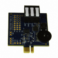
Manufacturer Part Number
TOOLSTICK560DC
Description
DAUGHTER CARD TOOLSTICK F560
Manufacturer
Silicon Laboratories Inc
Series
ToolStickr
Type
MCUr
Specifications of TOOLSTICK560DC
Contents
Daughter Card
Processor To Be Evaluated
C8051F55x, C8051F56x, C8051F57x
Interface Type
USB
Operating Supply Voltage
2.7 V to 3.6 V
Lead Free Status / RoHS Status
Lead free / RoHS Compliant
For Use With/related Products
C8051F55x, C8051F56x, C8051F57x
For Use With
336-1345 - TOOLSTICK BASE ADAPTER336-1182 - ADAPTER USB DEBUG FOR C8051FXXX
Lead Free Status / Rohs Status
Lead free / RoHS Compliant
Other names
336-1719


Post-Tracking Mode is selected when AD0TM is set to 01b. A programmable tracking time based on
AD0TK is started immediately following the convert start signal. Conversions are started after the pro-
grammed tracking time ends. After a conversion is complete, ADC0 does not track the input. Rather, the
sampling capacitor remains disconnected from the input making the input pin high-impedance until the
next convert start signal.
Dual-Tracking Mode is selected when AD0TM is set to 11b. A programmable tracking time based on
AD0TK is started immediately following the convert start signal. Conversions are started after the pro-
grammed tracking time ends. After a conversion is complete, ADC0 tracks continuously until the next con-
version is started.
Depending on the output connected to the ADC input, additional tracking time, more than is specified in
Table 5.9, may be required after changing MUX settings. See the settling time requirements described in
Section “6.2.1. Settling Time Requirements” on page 52.
6.1.3. Timing
ADC0 has a maximum conversion speed specified in Table 5.9. ADC0 is clocked from the ADC0 Subsys-
tem Clock (FCLK). The source of FCLK is selected based on the BURSTEN bit. When BURSTEN is
logic 0, FCLK is derived from the current system clock. When BURSTEN is logic 1, FCLK is derived from
the Burst Mode Oscillator, an independent clock source with a maximum frequency of 25 MHz.
When ADC0 is performing a conversion, it requires a clock source that is typically slower than FCLK. The
ADC0 SAR conversion clock (SAR clock) is a divided version of FCLK. The divide ratio can be configured
using the AD0SC bits in the ADC0CF register. The maximum SAR clock frequency is listed in Table 5.9.
ADC0 can be in one of three states at any given time: tracking, converting, or idle. Tracking time depends
on the tracking mode selected. For Pre-Tracking Mode, tracking is managed by software and ADC0 starts
conversions immediately following the convert start signal. For Post-Tracking and Dual-Tracking Modes,
the tracking time after the convert start signal is equal to the value determined by the AD0TK bits plus 2
FCLK cycles. Tracking is immediately followed by a conversion. The ADC0 conversion time is always 13
SAR clock cycles plus an additional 2 FCLK cycles to start and complete a conversion. Figure 6.3 shows
timing diagrams for a conversion in Pre-Tracking Mode and tracking plus conversion in Post-Tracking or
Dual-Tracking Mode. In this example, repeat count is set to one.
Dual-Tracking
Post-Tracking
Convert Start
Pre-Tracking
AD0TM = 10
AD0TM = 11
AD0TM= 01
Track
Track
Idle
Track
Track
Figure 6.2. ADC0 Tracking Modes
Convert
Rev. 1.1
Convert
Convert
C8051F55x/56x/57x
Track
Track
Idle
Track
Track
Convert ...
Convert..
Convert..
49
Related parts for TOOLSTICK560DC
Image
Part Number
Description
Manufacturer
Datasheet
Request
R

Part Number:
Description:
KIT TOOL EVAL SYS IN A USB STICK
Manufacturer:
Silicon Laboratories Inc
Datasheet:

Part Number:
Description:
TOOLSTICK DEBUG ADAPTER
Manufacturer:
Silicon Laboratories Inc
Datasheet:

Part Number:
Description:
TOOLSTICK BASE ADAPTER
Manufacturer:
Silicon Laboratories Inc
Datasheet:

Part Number:
Description:
TOOLSTICK DAUGHTER CARD
Manufacturer:
Silicon Laboratories Inc
Datasheet:

Part Number:
Description:
TOOLSTICK DAUGHTER CARD
Manufacturer:
Silicon Laboratories Inc
Datasheet:

Part Number:
Description:
TOOLSTICK DAUGHTER CARD
Manufacturer:
Silicon Laboratories Inc
Datasheet:

Part Number:
Description:
TOOLSTICK PROGRAMMING ADAPTER
Manufacturer:
Silicon Laboratories Inc
Datasheet:

Part Number:
Description:
TOOLSTICK DAUGHTER CARD
Manufacturer:
Silicon Laboratories Inc
Datasheet:

Part Number:
Description:
KIT STARTER TOOLSTICK
Manufacturer:
Silicon Laboratories Inc
Datasheet:

Part Number:
Description:
KIT UNIVERSITY TOOLSTICK STARTER
Manufacturer:
Silicon Laboratories Inc
Datasheet:

Part Number:
Description:
DAUGHTER CARD TOOLSTICK F330
Manufacturer:
Silicon Laboratories Inc
Datasheet:

Part Number:
Description:
CARD DAUGHTER UNIVRSTY TOOLSTICK
Manufacturer:
Silicon Laboratories Inc
Datasheet:

Part Number:
Description:
DAUGHTER CARD TOOLSTICK F582
Manufacturer:
Silicon Laboratories Inc
Datasheet:

Part Number:
Description:
DAUGHTER CARD TOOLSTICK F500
Manufacturer:
Silicon Laboratories Inc
Datasheet:

Part Number:
Description:
DAUGHTER CARD TOOLSTICK F540
Manufacturer:
Silicon Laboratories Inc
Datasheet: