EDOSK2674 Renesas Electronics America, EDOSK2674 Datasheet - Page 24
EDOSK2674
Manufacturer Part Number
EDOSK2674
Description
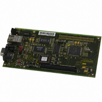
DEV EVALUATION KIT H8S/2674
Manufacturer
Renesas Electronics America
Series
H8®r
Type
MCUr
Datasheet
1.EDOSK2674.pdf
(38 pages)
Specifications of EDOSK2674
Contents
EDOSK (Evaluation Development Operating System Kit) Board
For Use With/related Products
H8S/2674R
Lead Free Status / RoHS Status
Contains lead / RoHS non-compliant


WTCRBH (H’FFFEC4) = H’71
Bit No
Bit Name
Initial Value
Area 3 has 7 program wait states inserted.
SDRAM has a CAS Latency of 2.
WTCRBL (H’FFFEC5) = H’23 (BOOT) or H’22 (NORMAL)
Bit No
Bit Name
Initial Value
Area 1 has 2 program wait states inserted.
In BOOT mode, area 0 has 3 program wait states inserted.
In NORMAL mode area 0 has 2 program wait states inserted.
Read Strobe Timing Control Register:
RDNCR (H’FFFEC6) = H’00
Bit No
Bit Name
Initial Value
In all areas the /RD signal is negated at the end of the read cycle.
CS assertion Period Control Registers:
CSACRH (H’FFFEC8) = H’80
Bit No
Bit Name
Initial Value
In area 7 basic bus interface access, the /CSn and address assertion period (T
CSACRL (H’FFFEC9) = H’80
Bit No
Bit Name
Initial Value
In area 7 basic bus interface access, the /CSn and address assertion period (T
15
Reserved
0
7
Reserved
0
7
RDN7
0
7
CSXH7
1
7
CSXT7
1
W32
14
1
6
W12
0
6
RDN
0
6
CSXH6
0
6
CSXT6
0
13
W31
1
5
W11
1
5
RDN
0
5
CSXH5
0
5
CSXT5
0
12
W30
1
4
W10
0
4
0
4
CSXH4
0
4
CSXT4
0
RDN
11
Reserved
0
3
Reserved
0
3
RDN
0
3
CSXH3
0
3
CSXT3
0
h
t
) is extended.
) is extended.
10
W22
0
2
W12
0
2
RDN
0
2
CSXH2
0
2
CSXT2
0
9
W21
0
1
W11
1
1
RDN
0
1
CSXH1
0
1
CSXT1
0
8
W20
1
0
W10
1 or 0
0
RDN
0
0
CSXH0
0
0
CSXT0
0
24
Related parts for EDOSK2674
Image
Part Number
Description
Manufacturer
Datasheet
Request
R

Part Number:
Description:
KIT STARTER FOR M16C/29
Manufacturer:
Renesas Electronics America
Datasheet:

Part Number:
Description:
KIT STARTER FOR R8C/2D
Manufacturer:
Renesas Electronics America
Datasheet:

Part Number:
Description:
R0K33062P STARTER KIT
Manufacturer:
Renesas Electronics America
Datasheet:

Part Number:
Description:
KIT STARTER FOR R8C/23 E8A
Manufacturer:
Renesas Electronics America
Datasheet:

Part Number:
Description:
KIT STARTER FOR R8C/25
Manufacturer:
Renesas Electronics America
Datasheet:

Part Number:
Description:
KIT STARTER H8S2456 SHARPE DSPLY
Manufacturer:
Renesas Electronics America
Datasheet:

Part Number:
Description:
KIT STARTER FOR R8C38C
Manufacturer:
Renesas Electronics America
Datasheet:

Part Number:
Description:
KIT STARTER FOR R8C35C
Manufacturer:
Renesas Electronics America
Datasheet:

Part Number:
Description:
KIT STARTER FOR R8CL3AC+LCD APPS
Manufacturer:
Renesas Electronics America
Datasheet:
Part Number:
Description:
KIT STARTER FOR RX610
Manufacturer:
Renesas Electronics America
Datasheet:

Part Number:
Description:
KIT STARTER FOR R32C/118
Manufacturer:
Renesas Electronics America
Datasheet:

Part Number:
Description:
KIT DEV RSK-R8C/26-29
Manufacturer:
Renesas Electronics America
Datasheet:

Part Number:
Description:
KIT STARTER FOR SH7124
Manufacturer:
Renesas Electronics America
Datasheet:

Part Number:
Description:
KIT STARTER FOR H8SX/1622
Manufacturer:
Renesas Electronics America
Datasheet:

Part Number:
Description:
KIT DEV FOR SH7203
Manufacturer:
Renesas Electronics America
Datasheet: