EDOSK2674 Renesas Electronics America, EDOSK2674 Datasheet - Page 31
EDOSK2674
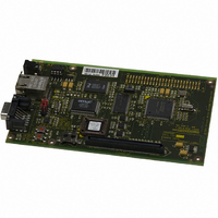
Manufacturer Part Number
EDOSK2674
Description
DEV EVALUATION KIT H8S/2674
Manufacturer
Renesas Electronics America
Series
H8®r
Type
MCUr
Datasheet
1.EDOSK2674.pdf
(38 pages)
Specifications of EDOSK2674
Contents
EDOSK (Evaluation Development Operating System Kit) Board
For Use With/related Products
H8S/2674R
Lead Free Status / RoHS Status
Contains lead / RoHS non-compliant


Enable SDRAM CS.
Port 3 Register:
PORT3 (H’FFFF52)
Bit No
Bit Name
Initial Value
Read only, value determined by the states of pins P35 to P30.
Port 3 Open Drain Control Register:
P3ODR (H’FFFE3C) = H’06
Bit No
Bit Name
Initial Value
I2C signals are NMOS open-drain
Port A Data Direction Register:
PADDR (H’FFFE29) = H’FF
Bit No
Bit Name
Initial Value
The individual bits of PADDR specify input or output for the pins of port A – ‘0’ input, ‘1’ output.
Port F Data Direction Register:
PFDDR (H’FFFE2E) = H’FE
Bit No
Bit Name
Initial Value
The individual bits of PFDDR specify input or output for the pins of port F – ‘0’ input, ‘1’ output.
Set all as outputs except PF0 (WAITn)
Port G Data Direction Register:
PGDDR (H’FFFE2F) = H’0F
Bit No
Bit Name
Initial Value
The individual bits of PGDDR specify input or output for the pins of port G – ‘0’ input, ‘1’ output.
7
Reserved
0
7
Reserved
0
7
PADDR
1
7
PFDDR
1
7
Reserved
0
Reserved
0
6
6
Reserved
0
6
PADDR
1
6
PFDDR
1
6
PGDDR
0
5
P35
X
5
P35ODR
0
5
PADDR
1
5
PFDDR
1
5
PGDDR
0
4
P34
X
4
0
4
PADDR
1
4
PFDDR
1
4
0
P34ODR
PGDDR
3
P33
X
3
P33ODR
0
3
PADDR
1
3
PFDDR
1
3
PGDDR
1
2
P32
X
2
P32ODR
1
2
PADDR
1
2
PFDDR
1
2
PGDDR
1
1
P31
X
1
P31ODR
1
1
PADDR
1
1
PFDDR
1
1
PGDDR
1
0
P30
X
0
P30ODR
0
0
PADDR
1
0
PFDDR
0
0
PGDDR
1
31
Related parts for EDOSK2674
Image
Part Number
Description
Manufacturer
Datasheet
Request
R

Part Number:
Description:
KIT STARTER FOR M16C/29
Manufacturer:
Renesas Electronics America
Datasheet:

Part Number:
Description:
KIT STARTER FOR R8C/2D
Manufacturer:
Renesas Electronics America
Datasheet:

Part Number:
Description:
R0K33062P STARTER KIT
Manufacturer:
Renesas Electronics America
Datasheet:

Part Number:
Description:
KIT STARTER FOR R8C/23 E8A
Manufacturer:
Renesas Electronics America
Datasheet:

Part Number:
Description:
KIT STARTER FOR R8C/25
Manufacturer:
Renesas Electronics America
Datasheet:

Part Number:
Description:
KIT STARTER H8S2456 SHARPE DSPLY
Manufacturer:
Renesas Electronics America
Datasheet:

Part Number:
Description:
KIT STARTER FOR R8C38C
Manufacturer:
Renesas Electronics America
Datasheet:

Part Number:
Description:
KIT STARTER FOR R8C35C
Manufacturer:
Renesas Electronics America
Datasheet:

Part Number:
Description:
KIT STARTER FOR R8CL3AC+LCD APPS
Manufacturer:
Renesas Electronics America
Datasheet:
Part Number:
Description:
KIT STARTER FOR RX610
Manufacturer:
Renesas Electronics America
Datasheet:

Part Number:
Description:
KIT STARTER FOR R32C/118
Manufacturer:
Renesas Electronics America
Datasheet:

Part Number:
Description:
KIT DEV RSK-R8C/26-29
Manufacturer:
Renesas Electronics America
Datasheet:

Part Number:
Description:
KIT STARTER FOR SH7124
Manufacturer:
Renesas Electronics America
Datasheet:

Part Number:
Description:
KIT STARTER FOR H8SX/1622
Manufacturer:
Renesas Electronics America
Datasheet:

Part Number:
Description:
KIT DEV FOR SH7203
Manufacturer:
Renesas Electronics America
Datasheet: