MPC8572DS Freescale Semiconductor, MPC8572DS Datasheet - Page 68
MPC8572DS
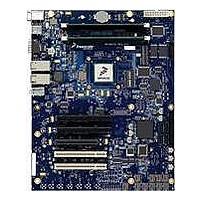
Manufacturer Part Number
MPC8572DS
Description
KIT MPU POWERQUICC III
Manufacturer
Freescale Semiconductor
Series
PowerQUICC III™r
Type
MPUr
Specifications of MPC8572DS
Contents
Board
Data Rate
10 Mbps to 100 Mbps
Memory Type
Flash, DDR, DDR2, DDR3, SDRAM
Interface Type
I2C, Ethernet
Operating Voltage
3.3 V
Data Bus Width
32 bit
Product
Development Tools
Silicon Manufacturer
Freescale
Core Architecture
Power Architecture
Core Sub-architecture
PowerQUICC
Silicon Core Number
MPC85xx
Silicon Family Name
PowerQUICC III
Rohs Compliant
Yes
For Use With/related Products
MPC8572E
Lead Free Status / RoHS Status
Lead free / RoHS Compliant


I
13.2
Table 55
68
At recommended operating conditions with OV
2
SCL clock frequency
Low period of the SCL clock
High period of the SCL clock
Setup time for a repeated START condition
Hold time (repeated) START condition (after this period, the first
clock pulse is generated)
Data setup time
Data input hold time:
Data output delay time
Setup time for STOP condition
Bus free time between a STOP and START condition
Noise margin at the LOW level for each connected device
(including hysteresis)
Noise margin at the HIGH level for each connected device
(including hysteresis)
Capacitive load for each bus line
Notes:
1.The symbols used for timing specifications herein follow the pattern t
2. As a transmitter, the MPC8572E provides a delay time of at least 300 ns for the SDA signal (referred to the VIHmin of the
3.The maximum t
4. The requirements for I
C
inputs and t
with respect to the time data input signals (D) reach the valid state (V) relative to the t
(H) state or setup time. Also, t
(S) went invalid (X) relative to the t
timing (I2) for the time that the data with respect to the STOP condition (P) reaching the valid state (V) relative to the t
reference (K) going to the high (H) state or setup time.
SCL signal) to bridge the undefined region of the falling edge of SCL to avoid unintended generation of START or STOP
condition. When the MPC8572E acts as the I2C bus master while transmitting, the MPC8572E drives both SCL and SDA.
As long as the load on SCL and SDA are balanced, the MPC8572E would not cause unintended generation of START or
STOP condition. Therefore, the 300 ns SDA output delay time is not a concern. If, under some rare condition, the 300 ns SDA
output delay time is required for the MPC8572E as transmitter, application note AN2919 referred to in note 4 below is
recommended.
the I
2
C Frequency Divider Ratio for SCL .
provides the AC timing parameters for the I
I
2
C AC Electrical Specifications
(first two letters of functional block)(reference)(state)(signal)(state)
I2OVKL
MPC8572E PowerQUICC III Integrated Processor Hardware Specifications, Rev. 5
has only to be met if the device does not stretch the LOW period (t
2
C frequency calculation must be followed. Refer to Freescale application note AN2919, Determining
Parameter
I2SXKL
I2C
CBUS compatible masters
Table 55. I
symbolizes I
clock reference (K) going to the low (L) state or hold time. Also, t
DD
of 3.3 V ± 5%. All values refer to V
I
2
C bus devices
2
2
C AC Electrical Specifications
C timing (I2) for the time that the data with respect to the START condition
2
C interfaces.
for outputs. For example, t
Symbol
t
t
t
t
t
t
t
I2PVKH
(first two letters of functional block)(signal)(state)(reference)(state)
I2SVKH
I2DVKH
I2KHDX
I2SXKL
I2DXKL
I2OVKL
t
t
V
V
f
I2CH
I2CL
Cb
I2C
NH
NL
IH
1
(min) and V
0.1 × OV
0.2 × OV
I2C
IL
Min
100
1.3
0.6
0.6
0.6
0.6
1.3
(max) levels (see
—
0
—
—
0
clock reference (K) going to the high
2
I2CL
I2DVKH
DD
DD
) of the SCL signal.
symbolizes I
Freescale Semiconductor
I2PVKH
Table
Max
0.9
400
400
—
—
—
—
—
—
—
—
—
—
—
3
2).
symbolizes I
2
C timing (I2)
I2C
kHz
Unit
clock
pF
μs
μs
μs
μs
ns
μs
μs
μs
μs
V
V
for
2
4
C
Related parts for MPC8572DS
Image
Part Number
Description
Manufacturer
Datasheet
Request
R

Part Number:
Description:
Manufacturer:
Freescale Semiconductor, Inc
Datasheet:
Part Number:
Description:
Manufacturer:
Freescale Semiconductor, Inc
Datasheet:
Part Number:
Description:
Manufacturer:
Freescale Semiconductor, Inc
Datasheet:
Part Number:
Description:
Manufacturer:
Freescale Semiconductor, Inc
Datasheet:
Part Number:
Description:
Manufacturer:
Freescale Semiconductor, Inc
Datasheet:
Part Number:
Description:
Manufacturer:
Freescale Semiconductor, Inc
Datasheet:
Part Number:
Description:
Manufacturer:
Freescale Semiconductor, Inc
Datasheet:
Part Number:
Description:
Manufacturer:
Freescale Semiconductor, Inc
Datasheet:
Part Number:
Description:
Manufacturer:
Freescale Semiconductor, Inc
Datasheet:
Part Number:
Description:
Manufacturer:
Freescale Semiconductor, Inc
Datasheet:
Part Number:
Description:
Manufacturer:
Freescale Semiconductor, Inc
Datasheet:
Part Number:
Description:
Manufacturer:
Freescale Semiconductor, Inc
Datasheet:
Part Number:
Description:
Manufacturer:
Freescale Semiconductor, Inc
Datasheet:
Part Number:
Description:
Manufacturer:
Freescale Semiconductor, Inc
Datasheet:
Part Number:
Description:
Manufacturer:
Freescale Semiconductor, Inc
Datasheet: