EVAL-AD7856CB Analog Devices Inc, EVAL-AD7856CB Datasheet - Page 14
EVAL-AD7856CB
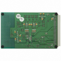
Manufacturer Part Number
EVAL-AD7856CB
Description
BOARD EVAL FOR AD7856
Manufacturer
Analog Devices Inc
Datasheet
1.AD7856ARSZ-REEL7.pdf
(32 pages)
Specifications of EVAL-AD7856CB
Lead Free Status / RoHS Status
Contains lead / RoHS non-compliant


AD7856
Adjusting the Offset Calibration Register
The offset calibration register contains 16 bits, two leading zeros
and 14 data bits. By changing the contents of the offset register
different amounts of offset on the analog input signal can be
compensated for. Increasing the number in the offset calibration
register compensates for negative offset on the analog input
signal, and decreasing the number in the offset calibration regis-
ter compensates for positive offset on the analog input signal.
The default value of the offset calibration register is approxi-
mately 0010 0000 0000 0000. This is not an exact value, but
the value in the offset register should be close to this value. Each
Figure 9. Flowchart for Reading from the Calibration
Registers
WRITE TO CONTROL REGISTER SETTING STCAL = 0, RDSLT1 = 1,
RDSLT0 = 0, AND CALSLT1, CALSLT0 = 00, 01, 10, 11
AUTOMATICALLY INCREMENTED
CAL REGISTER POINTER IS
CAL REGISTER POINTER IS
AUTOMATICALLY RESET
READ CAL REGISTER
OPERATION
REGISTER
FINISHED
START
ABORT
READ
LAST
OR
?
YES
NO
–14–
of the 14 data bits in the offset register is binary weighted: the
MSB has a weighting of 5% of the reference voltage, the MSB-1
has a weighting of 2.5%, the MSB-2 has a weighting of 1.25%,
and so on down to the LSB, which has a weighting of 0.0006%.
This gives a resolution of approximately 0.0006% of V
More accurately the resolution is (0.05
offset that can be compensated for is 3.75% of the reference
voltage but is typically 5%, which equates to 125 mV with a
2.5 V reference and 250 mV with a 5 V reference.
Q. If a +20 mV offset is present in the analog input signal and the
A. 2.5 V reference implies that the resolution in the offset regis-
This method of compensating for offset in the analog input
signal allows for fine tuning the offset compensation. If the
offset on the analog input signal is known, there will be no need
to apply the offset voltage to the analog input pins and do a
system calibration. The offset compensation can take place in
software.
Adjusting the Gain Calibration Register
The gain calibration register contains 16 bits, two leading 0s
and 14 data bits. The data bits are binary weighted as in the
offset calibration register. The gain register value is effectively
multiplied by the analog input to scale the conversion result
over the full range. Increasing the gain register compensates for
a smaller analog input range and decreasing the gain register
compensates for a larger input range. The maximum analog
input range for which the gain register can compensate is
1.01875 times the reference voltage; the minimum input range
is 0.98125 times the reference voltage.
0.015 mV, with a 2.5 V reference. The maximum specified
reference voltage is 2.5 V, what code needs to be written to the
offset register to compensate for the offset?
ter is 5%
1310.72; rounding to the nearest number gives 1311. In
binary terms this is 0101 0001 1111. Therefore, decrease the
offset register by 0101 0001 1111.
2.5 V/2
13
= 0.015 mV. +20 mV/0.015 mV =
V
REF
)/2
13
volts =
REV. A
REF
.
Related parts for EVAL-AD7856CB
Image
Part Number
Description
Manufacturer
Datasheet
Request
R

Part Number:
Description:
ENERCHIP CC EVAL KIT
Manufacturer:
Cymbet Corporation
Datasheet:

Part Number:
Description:
BOARD EVAL FOR AD976
Manufacturer:
Analog Devices Inc
Datasheet:

Part Number:
Description:
BOARD EVAL FOR ADXL345
Manufacturer:
Analog Devices Inc
Datasheet:

Part Number:
Description:
ENERCHIP CC SEH EVAL KIT
Manufacturer:
Cymbet Corporation
Datasheet:

Part Number:
Description:
ENERCHIP EP ENERGY HARVEST EVAL
Manufacturer:
Cymbet Corporation
Datasheet:

Part Number:
Description:
EVAL BOARD FOR TW6864-LB2-GR
Manufacturer:
Intersil
Datasheet:
Part Number:
Description:
EVAL BOARD FOR TW8816-LB3-GR
Manufacturer:
Intersil
Datasheet:
Part Number:
Description:
EVAL BOARD FOR TW8817-TA3-GRS
Manufacturer:
Intersil
Datasheet:

Part Number:
Description:
EVALUATION MODULE FOR ADUM4160
Manufacturer:
Analog Devices Inc
Datasheet:

Part Number:
Description:
BOARD EVALUATION ADCMP581BCP
Manufacturer:
Analog Devices Inc
Datasheet:
Part Number:
Description:
BOARD EVALUATION ADM1041
Manufacturer:
Analog Devices Inc
Datasheet:

Part Number:
Description:
EVAL BOARD FOR STM32F107VCT
Manufacturer:
STMicroelectronics
Datasheet:
Part Number:
Description:
BOARD EVAL FOR AD1954
Manufacturer:
Analog Devices Inc
Datasheet:
Part Number:
Description:
BOARD EVAL FOR AD1955
Manufacturer:
Analog Devices Inc
Datasheet:

Part Number:
Description:
BOARD EVAL FOR AD7655
Manufacturer:
Analog Devices Inc
Datasheet: