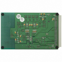
EVAL-AD7856CB Analog Devices Inc, EVAL-AD7856CB Datasheet - Page 2

EVAL-AD7856CB
Manufacturer Part Number
EVAL-AD7856CB
Description
BOARD EVAL FOR AD7856
Manufacturer
Analog Devices Inc
Datasheet
1.AD7856ARSZ-REEL7.pdf
(32 pages)
Specifications of EVAL-AD7856CB
Lead Free Status / RoHS Status
Contains lead / RoHS non-compliant
AD7856–SPECIFICATIONS
REF
tions apply for Mode 2 operation, standard 3-wire SPI interface; refer to Detailed Timing section for Mode 1 Specifications.
Parameter
DYNAMIC PERFORMANCE
DC ACCURACY
ANALOG INPUT
REFERENCE INPUT/OUTPUT
LOGIC INPUTS
LOGIC OUTPUTS
CONVERSION RATE
Signal to Noise + Distortion Ratio
Total Harmonic Distortion (THD)
Peak Harmonic or Spurious Noise
Intermodulation Distortion (IMD)
Resolution
Integral Nonlinearity
Differential Nonlinearity
Offset Error
Offset Error Match
Positive Full-Scale Error
Positive Full-Scale Error Match
Input Voltage Ranges
Leakage Current
Input Capacitance
REF
Input Impedance
REF
REF
Input High Voltage, V
Input Low Voltage, V
Input Current, I
Input Capacitance, C
Output High Voltage, V
Output Low Voltage, V
Floating-State Leakage Current
Floating-State Output Capacitance
Output Coding
Conversion Time
Track/Hold Acquisition Time
IN
Second Order Terms
Third Order Terms
Channel-to-Channel Isolation
/REF
IN
OUT
OUT
Input Voltage Range
OUT
Output Voltage
Tempco
= 4.096 V External Reference unless otherwise noted, SLEEP = Logic High; T
IN
IN
INL
INH
4
OL
OH
3
4
(SNR)
A Version
78
–86
–86
–86
–90
14
0 to V
20
4.096/V
150
3.696/4.496
20
V
0.4
10
V
0.4
10
3.5
0.33
–87
2
2
10
10
1
1
1
DD
DD
Straight (Natural) Binary
– 1.0
– 0.4
REF
DD
1, 2
1
K Version
78
–90
–90
0 to V
2.3/V
20
0.4
10
0.4
10
–86
–87
–90
14
20
150
3.696/4.496
V
V
5.25
0.5
A Grade: f
f
2
2
10
5
3
10
2
1
DD
1
DD
1
CLKIN
– 1.0
– 0.4
DD
REF
= 4 MHz, (0 C to +105 C), f
–2–
1
CLKIN
= 6 MHz, (–40 C to +105 C), f
Units
dB min
dB max
dB max
dB typ
dB typ
dB typ
Bits
LSB max
LSB typ
LSB max
LSB typ
LSB max
LSB typ
LSB max
LSB max
LSB typ
LSB max
Volts
pF typ
V min/max
k typ
V min/max
ppm/ C typ
V min
V max
pF max
V min
V max
pF max
A max
A max
A max
s max
s min
A
= T
Test Conditions/Comments
f
79.5 dB typ
–95 dB typ
fa = 9.983 kHz, fb = 10.05 kHz
fa = 9.983 kHz, fb = 10.05 kHz
V
Any Channel
4.096 V External Reference, V
Guaranteed No Missed Codes to 13 Bits.
i.e., AIN(+) – AIN(–) = 0 to V
Biased Up, but AIN(+) Cannot Go Below AIN(–)
Functional from 1.2 V
Resistor Connected to Internal Reference Node
Typically 10 nA, V
I
I
21 CLKIN Cycles
IN
–95 dB typ
SOURCE
SINK
IN
MIN
= 10 kHz
= 25 kHz
SAMPLE
= 0.8 mA
to T
= 200 A
MAX
= 102 kHz; (AV
, unless otherwise noted.) Specifica-
SAMPLE
IN
= 0 V or V
= 285 kHz; K Grade:
DD
= DV
DD
REF
DD
DD
= 5 V
, AIN(–) Can Be
= +5.0 V
REV. A
5%,


