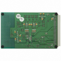
EVAL-AD7856CB Analog Devices Inc, EVAL-AD7856CB Datasheet - Page 3

EVAL-AD7856CB
Manufacturer Part Number
EVAL-AD7856CB
Description
BOARD EVAL FOR AD7856
Manufacturer
Analog Devices Inc
Datasheet
1.AD7856ARSZ-REEL7.pdf
(32 pages)
Specifications of EVAL-AD7856CB
Lead Free Status / RoHS Status
Contains lead / RoHS non-compliant
Parameter
POWER PERFORMANCE
SYSTEM CALIBRATION
NOTES
1
2
3
4
5
6
7
Specifications subject to change without notice.
REV. A
Temperature ranges as follows: A Version: –40 C to +105 C. K Version: 0 C to +105 C.
Specifications apply after calibration.
SNR calculation includes distortion and noise components.
Sample tested @ +25 C to ensure compliance.
All digital inputs @ DGND except for CONVST, SLEEP, CAL and SYNC @ DV
CLKIN @ DGND when external clock off. All digital inputs @ DGND except for CONVST, SLEEP, CAL, and SYNC @ DV
The Offset and Gain Calibration Spans are defined as the range of offset and gain errors that the AD7856 can calibrate. Note also that these are voltage spans and are
Analog inputs @ AGND.
not absolute voltages (i.e., the allowable system offset voltage presented at AIN(+) for the system offset error to be adjusted out will be AIN(–)
the allowable system full-scale voltage applied between AIN(+) and AIN(–) for the system full-scale voltage error to be adjusted out will be V
This is explained in more detail in the Calibration section of the data sheet.
AV
I
Normal Mode Power Dissipation
Sleep Mode Power Dissipation
Offset Calibration Span
Gain Calibration Span
DD
Normal Mode
Sleep Mode
With External Clock On
With External Clock Off
DD,
With External Clock On
With External Clock Off
DV
DD
6
5
7
7
A Version
+4.75/+5.25
17
30
400
5
200
89.25
52.5
26.25
+0.0375 V
+1.01875 V
1
REF
REF
/–0.0375 V
/–0.98125 V
K Version
+4.75/+5.25
17
10
500
5
200
89.25
52.5
26.25
–3–
REF
DD
1
REF
. No load on the digital outputs. Analog inputs @ AGND.
Units
V min/max
mA max
mW max
V max/min
V max/min
A typ
A typ
A max
A typ
W typ
W max
Test Conditions/Comments
AV
Full Power-Down. Power Management Bits in Con-
trol Register Set as PMGT1 = 1, PMGT0 = 0
Partial Power-Down. Power Management Bits in
Control Register Set as PMGT1 = 1, PMGT0 = 1
Typically 0.5 A. Full Power-Down. Power Manage-
ment. Bits in Control Register Set as PMGT1 = 1,
PMGT0 = 0
Partial Power-Down. Power Management Bits in
Control Register Set as PMGT1 = 1, PMGT0 = 1
V
V
V
Allowable Offset Voltage Span for Calibration
Allowable Full-Scale Voltage Span for Calibration
DD
DD
DD
DD
= 5.25 V. Typically 60 mW; SLEEP = V
= 5.25 V. SLEEP = 0 V
= 5.25 V. Typically 5.25 W; SLEEP = 0 V
= DV
DD
= 4.75 V to 5.25 V. Typically 12 mA
DD
. No load on the digital outputs.
REF
0.0375
0.01875
AD7856
V
REF
DD
V
, and
REF
).


