EVAL-AD7856CB Analog Devices Inc, EVAL-AD7856CB Datasheet - Page 25
EVAL-AD7856CB
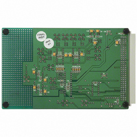
Manufacturer Part Number
EVAL-AD7856CB
Description
BOARD EVAL FOR AD7856
Manufacturer
Analog Devices Inc
Datasheet
1.AD7856ARSZ-REEL7.pdf
(32 pages)
Specifications of EVAL-AD7856CB
Lead Free Status / RoHS Status
Contains lead / RoHS non-compliant


Mode 2 (3-Wire SPI/QSPI Interface Mode)
This is the DEFAULT INTERFACE MODE.
In Figure 33 below we have the timing diagram for interface
Mode 2, which is the SPI/QSPI interface mode. Here the SYNC
input is active low and may be pulsed or permanently tied low.
If SYNC is permanently low, 16 clock pulses must be applied to
the SCLK pin for the part to operate correctly otherwise, with a
pulsed SYNC input, a continuous SCLK may be applied pro-
vided SYNC is low for only 16 SCLK cycles. In Figure 33 the
REV. A
Figure 33. SPI/QSPI Mode 2 Timing Diagram for Read/Write Operation with DIN Input
DOUT Output and SYNC Input
DOUT (O/P)
DIN (I/P)
POLARITY PIN LOGIC HIGH
SYNC (I/P)
SCLK (I/P)
THREE-
STATE
t
5
t
3
DB15
t
1
7
t
t
t
3
6
11
= –0.4
= 45/75ns MAX (A/K),
= 30ns MIN (NONCONTINUOUS SCLK), 30/0.4
DB15
t
6
t
DB14
SCLK
t
2
8
DB14
MIN (NONCONTINUOUS SCLK) –/+0.4
t
9
DB13
t
3
10
t
DB13
7
= 30/40ns MIN (A/K),
–25–
DB12
4
t
DB12
6
SYNC going low disables the three-state on the DOUT pin. The
first falling edge of the SCLK after the SYNC going low clocks
out the first leading zero on the DOUT pin. The DOUT pin is
three-stated again a time, t
the DIN pin the data input has to be set up a time, t
SCLK rising edge as the part samples the input data on the
SCLK rising edge in this case. If resetting the interface is re-
quired, the SYNC must be taken high and then low.
DB11
5
DB11
t
8
t
SCLK
= 20ns MIN,
t
t
8
DB10
SCLK
ns MIN/MAX (CONTINUOUS SCLK)
6
ns MIN/MAX (CONTINUOUS SCLK),
DB10
12
DB0
, after the SYNC goes high. With
16
DB0
t
11
THREE-
STATE
t
12
AD7856
7
, before the
Related parts for EVAL-AD7856CB
Image
Part Number
Description
Manufacturer
Datasheet
Request
R

Part Number:
Description:
ENERCHIP CC EVAL KIT
Manufacturer:
Cymbet Corporation
Datasheet:

Part Number:
Description:
BOARD EVAL FOR AD976
Manufacturer:
Analog Devices Inc
Datasheet:

Part Number:
Description:
BOARD EVAL FOR ADXL345
Manufacturer:
Analog Devices Inc
Datasheet:

Part Number:
Description:
ENERCHIP CC SEH EVAL KIT
Manufacturer:
Cymbet Corporation
Datasheet:

Part Number:
Description:
ENERCHIP EP ENERGY HARVEST EVAL
Manufacturer:
Cymbet Corporation
Datasheet:

Part Number:
Description:
EVAL BOARD FOR TW6864-LB2-GR
Manufacturer:
Intersil
Datasheet:
Part Number:
Description:
EVAL BOARD FOR TW8816-LB3-GR
Manufacturer:
Intersil
Datasheet:
Part Number:
Description:
EVAL BOARD FOR TW8817-TA3-GRS
Manufacturer:
Intersil
Datasheet:

Part Number:
Description:
EVALUATION MODULE FOR ADUM4160
Manufacturer:
Analog Devices Inc
Datasheet:

Part Number:
Description:
BOARD EVALUATION ADCMP581BCP
Manufacturer:
Analog Devices Inc
Datasheet:
Part Number:
Description:
BOARD EVALUATION ADM1041
Manufacturer:
Analog Devices Inc
Datasheet:

Part Number:
Description:
EVAL BOARD FOR STM32F107VCT
Manufacturer:
STMicroelectronics
Datasheet:
Part Number:
Description:
BOARD EVAL FOR AD1954
Manufacturer:
Analog Devices Inc
Datasheet:
Part Number:
Description:
BOARD EVAL FOR AD1955
Manufacturer:
Analog Devices Inc
Datasheet:

Part Number:
Description:
BOARD EVAL FOR AD7655
Manufacturer:
Analog Devices Inc
Datasheet: