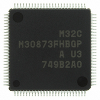
M30873FHBGP#U3 Renesas Electronics America, M30873FHBGP#U3 Datasheet - Page 460

M30873FHBGP#U3
Manufacturer Part Number
M30873FHBGP#U3
Description
IC M32C/87 MCU FLASH 100LQFP
Manufacturer
Renesas Electronics America
Series
M16C™ M32C/80r
Datasheet
1.M3087BFLGPU3.pdf
(629 pages)
Specifications of M30873FHBGP#U3
Core Processor
M32C/80
Core Size
16/32-Bit
Speed
32MHz
Connectivity
EBI/EMI, I²C, IEBus, IrDA, SIO, UART/USART
Peripherals
DMA, POR, PWM, WDT
Number Of I /o
85
Program Memory Size
384KB (384K x 8)
Program Memory Type
FLASH
Ram Size
24K x 8
Voltage - Supply (vcc/vdd)
3 V ~ 5.5 V
Data Converters
A/D 26x10b; D/A 2x8b
Oscillator Type
Internal
Operating Temperature
-40°C ~ 85°C
Package / Case
100-LQFP
For Use With
R0K330879S001BE - KIT DEV RSK M32C/87R0K330879S000BE - KIT DEV RSK M32C/87
Lead Free Status / RoHS Status
Lead free / RoHS Compliant
Eeprom Size
-
Available stocks
Company
Part Number
Manufacturer
Quantity
Price
- Current page: 460 of 629
- Download datasheet (16Mb)
M32C/87 Group (M32C/87, M32C/87A, M32C/87B)
REJ09B0180-0151 Rev.1.51 Jul 31, 2008
Page 436 of 587
Figure 23.27
CANi Global Mask Register Extended ID2
CANi Local Mask Register A Extended ID2
CANi Local Mask Register B Extended ID2
b7 b6 b5 b4
NOTES:
1. Registers CiGMR4, CiLMAR4, and CiLMBR4 can be accessed when the BANKSEL bit in the CiCTLR1 register is set to 1 (mask
2. Value is obtained by setting the SLEEP bit in the CiSLPR register to 1 (sleep mode exited) after reset, supplying the clock to the CAN
3. The C0LMAR4 register shares the same address with the C0MCTL4 register, and the C1LMAR4 register with the C1MCTL4 register.
4. The C0LMBR4 register shares the same address with the C0MCTL12 register, and the C1LMBR4 register with the C1MCTL12
register.
register selected).
module, and setting the BANKSEL bit to 1.
b3
b2
C0GMR4, C1GMR4, C0LMAR4, C1LMAR4, C0LMBR4, and C1LMBR4 Registers
b1
b0
Bit Symbol
(b7-b6)
EID0M
EID1M
EID2M
EID3M
EID4M
EID5M
C0GMR4, C1GMR4
C0LMAR4, C1LMAR4
C0LMBR4, C1LMBR4
Symbol
−
Extended ID0
Extended ID1
Extended ID2
Extended ID3
Extended ID4
Extended ID5
Unimplemented.
Write 0. Read as undefined value.
Bit Name
Address
022Ch, 02ACh
0234h, 02B4h
023Ch, 02BCh
(1)
(1)
(1)
(i = 0, 1)
0: ID not checked
1: ID checked
(3)
(4)
Function
After Reset
XX00 0000b
XX00 0000b
XX00 0000b
23. CAN Module
(2)
RW
RW
RW
RW
RW
RW
RW
−
Related parts for M30873FHBGP#U3
Image
Part Number
Description
Manufacturer
Datasheet
Request
R

Part Number:
Description:
KIT STARTER FOR M16C/29
Manufacturer:
Renesas Electronics America
Datasheet:

Part Number:
Description:
KIT STARTER FOR R8C/2D
Manufacturer:
Renesas Electronics America
Datasheet:

Part Number:
Description:
R0K33062P STARTER KIT
Manufacturer:
Renesas Electronics America
Datasheet:

Part Number:
Description:
KIT STARTER FOR R8C/23 E8A
Manufacturer:
Renesas Electronics America
Datasheet:

Part Number:
Description:
KIT STARTER FOR R8C/25
Manufacturer:
Renesas Electronics America
Datasheet:

Part Number:
Description:
KIT STARTER H8S2456 SHARPE DSPLY
Manufacturer:
Renesas Electronics America
Datasheet:

Part Number:
Description:
KIT STARTER FOR R8C38C
Manufacturer:
Renesas Electronics America
Datasheet:

Part Number:
Description:
KIT STARTER FOR R8C35C
Manufacturer:
Renesas Electronics America
Datasheet:

Part Number:
Description:
KIT STARTER FOR R8CL3AC+LCD APPS
Manufacturer:
Renesas Electronics America
Datasheet:

Part Number:
Description:
KIT STARTER FOR RX610
Manufacturer:
Renesas Electronics America
Datasheet:

Part Number:
Description:
KIT STARTER FOR R32C/118
Manufacturer:
Renesas Electronics America
Datasheet:

Part Number:
Description:
KIT DEV RSK-R8C/26-29
Manufacturer:
Renesas Electronics America
Datasheet:

Part Number:
Description:
KIT STARTER FOR SH7124
Manufacturer:
Renesas Electronics America
Datasheet:

Part Number:
Description:
KIT STARTER FOR H8SX/1622
Manufacturer:
Renesas Electronics America
Datasheet:

Part Number:
Description:
KIT DEV FOR SH7203
Manufacturer:
Renesas Electronics America
Datasheet:


