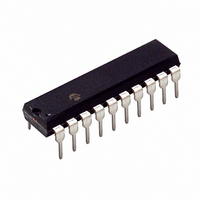
PIC16C770/P Microchip Technology, PIC16C770/P Datasheet - Page 112

PIC16C770/P
Manufacturer Part Number
PIC16C770/P
Description
IC MCU CMOS A/D 2K 20MHZ 20-DIP
Manufacturer
Microchip Technology
Series
PIC® 16Cr
Datasheets
1.PIC16C770-ISO.pdf
(220 pages)
2.PIC16C770-ISO.pdf
(6 pages)
3.PIC16C770-ISO.pdf
(8 pages)
Specifications of PIC16C770/P
Program Memory Type
OTP
Program Memory Size
3.5KB (2K x 14)
Package / Case
20-DIP (0.300", 7.62mm)
Core Processor
PIC
Core Size
8-Bit
Speed
20MHz
Connectivity
I²C, SPI
Peripherals
Brown-out Detect/Reset, POR, PWM, WDT
Number Of I /o
15
Ram Size
256 x 8
Voltage - Supply (vcc/vdd)
4 V ~ 5.5 V
Data Converters
A/D 6x12b
Oscillator Type
Internal
Operating Temperature
0°C ~ 70°C
Processor Series
PIC16C
Core
PIC
Data Bus Width
8 bit
Data Ram Size
256 B
Interface Type
I2C/SPI/SSP
Maximum Clock Frequency
20 MHz
Number Of Programmable I/os
16
Number Of Timers
3
Operating Supply Voltage
2.5 V to 5.5 V
Maximum Operating Temperature
+ 70 C
Mounting Style
Through Hole
3rd Party Development Tools
52715-96, 52716-328, 52717-734
Development Tools By Supplier
ICE2000
Minimum Operating Temperature
0 C
On-chip Adc
6-ch x 12-bit
Lead Free Status / RoHS Status
Lead free / RoHS Compliant
For Use With
DVA16XP200 - ADAPTER ICE 20DIP/SOIC/SSOPAC164028 - MODULE SKT PROMATEII 20SOIC/DIP
Eeprom Size
-
Lead Free Status / Rohs Status
Lead free / RoHS Compliant
- Current page: 112 of 220
- Download datasheet (4Mb)
PIC16C717/770/771
11.3
The A/D conversion cycle requires 13T
tling time, and 12 T
A/D conversion clock is software selected. If neither the
internal VRH nor VRL are used for the A/D converter,
the four possible options for T
TABLE 11-1:
DS41120B-page 110
External V
Analog Supply
Internal VRH or
VRL
Legend: Shaded cells are outside of recommended range.
Note 1: The A/D RC source has a typical T
A/D Reference
• 2 T
• 8 T
• 32 T
• A/D RC oscillator
Source
2: These values violate the minimum required T
3: For faster conversion times, the selection of another clock source is recommended.
4: When the device frequency is greater than 1 MHz, the A/D RC clock source is only recommended if the conversion will be
5: A/D RC clock source has a typical T
Selecting the A/D Conversion
Clock
OSC
OSC
performed during SLEEP.
REF
OSC
or
T
AD
2 T
8 T
32 T
A/D RC
16 T
64 T
256 T
A/D RC
AD
Operation
A/D Clock Source (T
for conversion. The source of the
OSC
OSC
vs. DEVICE OPERATING FREQUENCIES
OSC
OSC
OSC
OSC
AD
are:
ADCS<1:0>
AD
00
01
10
00
01
10
11
11
: 1 T
AD
AD
AD
time of 4 s for V
AD
time of 32 s for V
)
for set-
AD
16 - 48 s
2 - 6 s
time.
100 ns
400 ns
800 ns
3.2 s
20 MHz
12.8 s
1.6 s
DD
(1,4)
(2)
(2)
(2)
(2)
(4,5)
DD
> 3.0V.
If the VRH or VRL are used for the A/D converter refer-
ence, then the T
increased by a factor of 8.
For correct A/D conversions, the A/D conversion clock
(T
of 1.6 s. Table 11-1 shows the resultant T
derived from the device operating frequencies and the
A/D clock source selected.
The ADIF bit is set on the rising edge of the 14th T
The GO/DONE bit is cleared on the falling edge of the
14th T
> 3.0V.
AD
) must be selected to ensure a minimum T
16 - 48 s
2 - 6 s
AD
51.2 s
400 ns
6.4 s
3.2 s
12.8 s
5 MHz
1.6 s
.
Device Frequency
(3)
(1,4)
(2)
(2)
(3)
(4,5)
AD
16 - 48 s
2 - 6 s
requirement is automatically
500 ns
8.0 s
64 s
4 MHz
4 s
2.0 s
2002 Microchip Technology Inc.
16 s
(2)
(3)
(1,4)
(3)
(2)
(4,5)
16 - 48 s
2 - 6 s
204.8 s
1.25 MHz
25.6 s
51.2 s
12.8 s
1.6 s
6.4 s
AD
AD
(1,4)
(3)
(3)
times
(3)
(4,5)
time
AD
.
Related parts for PIC16C770/P
Image
Part Number
Description
Manufacturer
Datasheet
Request
R

Part Number:
Description:
IC, 8BIT MCU, PIC16C, 40MHZ, DIP-18
Manufacturer:
Microchip Technology
Datasheet:

Part Number:
Description:
IC, 8BIT MCU, PIC16C, 4MHZ, DIP-28
Manufacturer:
Microchip Technology
Datasheet:

Part Number:
Description:
IC, 8BIT MCU, PIC16C, 4MHZ, DIP-28
Manufacturer:
Microchip Technology
Datasheet:

Part Number:
Description:
IC, 8BIT MCU, PIC16C, 4MHZ, DIP-40
Manufacturer:
Microchip Technology
Datasheet:

Part Number:
Description:
SURFACE MOUNT POWER INDUCTORS
Manufacturer:
RCD [RCD COMPONENTS INC.]
Datasheet:

Part Number:
Description:
Manufacturer:
Microchip Technology Inc.
Datasheet:

Part Number:
Description:
Manufacturer:
Microchip Technology Inc.
Datasheet:

Part Number:
Description:
Manufacturer:
Microchip Technology Inc.
Datasheet:

Part Number:
Description:
Manufacturer:
Microchip Technology Inc.
Datasheet:

Part Number:
Description:
Manufacturer:
Microchip Technology Inc.
Datasheet:

Part Number:
Description:
Manufacturer:
Microchip Technology Inc.
Datasheet:


