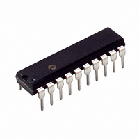
PIC16C770/P Microchip Technology, PIC16C770/P Datasheet - Page 156

PIC16C770/P
Manufacturer Part Number
PIC16C770/P
Description
IC MCU CMOS A/D 2K 20MHZ 20-DIP
Manufacturer
Microchip Technology
Series
PIC® 16Cr
Datasheets
1.PIC16C770-ISO.pdf
(220 pages)
2.PIC16C770-ISO.pdf
(6 pages)
3.PIC16C770-ISO.pdf
(8 pages)
Specifications of PIC16C770/P
Program Memory Type
OTP
Program Memory Size
3.5KB (2K x 14)
Package / Case
20-DIP (0.300", 7.62mm)
Core Processor
PIC
Core Size
8-Bit
Speed
20MHz
Connectivity
I²C, SPI
Peripherals
Brown-out Detect/Reset, POR, PWM, WDT
Number Of I /o
15
Ram Size
256 x 8
Voltage - Supply (vcc/vdd)
4 V ~ 5.5 V
Data Converters
A/D 6x12b
Oscillator Type
Internal
Operating Temperature
0°C ~ 70°C
Processor Series
PIC16C
Core
PIC
Data Bus Width
8 bit
Data Ram Size
256 B
Interface Type
I2C/SPI/SSP
Maximum Clock Frequency
20 MHz
Number Of Programmable I/os
16
Number Of Timers
3
Operating Supply Voltage
2.5 V to 5.5 V
Maximum Operating Temperature
+ 70 C
Mounting Style
Through Hole
3rd Party Development Tools
52715-96, 52716-328, 52717-734
Development Tools By Supplier
ICE2000
Minimum Operating Temperature
0 C
On-chip Adc
6-ch x 12-bit
Lead Free Status / RoHS Status
Lead free / RoHS Compliant
For Use With
DVA16XP200 - ADAPTER ICE 20DIP/SOIC/SSOPAC164028 - MODULE SKT PROMATEII 20SOIC/DIP
Eeprom Size
-
Lead Free Status / Rohs Status
Lead free / RoHS Compliant
- Current page: 156 of 220
- Download datasheet (4Mb)
PIC16C717/770/771
15.2
DS41120B-page 154
DC CHARACTERISTICS
D030
D030A
D031
D032
D033
D040
D040A
D041
D042
D042A
D070
D060
D060A
D061
D063
D080
D090
D150*
D100
D101
D102
Note 1: The leakage current on the MCLR pin is strongly dependent on the applied voltage level. The specified levels
Param.
No.
*
† Data in “Typ” column is at 5V, 25 C unless otherwise stated. These parameters are for design guidance only
2: Negative current is defined as current sourced by the pin.
I
DC Characteristics: PIC16C717/770/771 & PIC16LC717/770/771 (Commercial,
Industrial, Extended)
C
C
Sym
COS
These parameters are characterized but not tested.
and are not tested.
represent normal operating conditions. Higher leakage current may be measured at different input voltages.
PURB
V
V
V
C
V
V
C2
C
VRH
I
I
VRL
OH
OD
OL
IL
IL
IL
IH
IO
B
Input Low Voltage
I/O ports
MCLR
OSC1 (in XT, HS, LP and EC)
Input High Voltage
I/O ports
MCLR
OSC1 (XT, HS, LP and EC)
PORTB weak pull-up current
per pin
Input Leakage Current
I/O ports (with digital functions)
I/O ports (with analog func-
tions)
RA5/MCLR/V
OSC1
Output Low Voltage
I/O ports
Output High Voltage
I/O ports
Open Drain High Voltage
Capacitive Loading Specs on
Output Pins*
OSC2 pin
All I/O pins and OSC2 (in RC
mode) SCL, SDA in I
V
V
RH
RL
with TTL buffer
with Schmitt Trigger buffer
with TTL buffer
with Schmitt Trigger buffer
pin
pin
Characteristic
(2)
PP
2
C mode
(1,2)
Standard Operating Conditions (unless otherwise stated)
Operating temperature
Operating voltage V
Section 15.2.
(0.25V
V
+ 0.8V)
0.8V
0.8V
0.7V
DD
Min
V
V
V
V
V
2.0
50
—
—
—
—
—
—
—
—
—
—
—
SS
SS
SS
SS
SS
- 0.7
DD
DD
DD
DD
Typ†
250
—
—
—
—
—
—
—
—
—
—
—
—
—
—
—
—
—
—
—
—
—
—
—
0.15V
0.2V
0.2V
0.3V
0.8V
Max
10.5
V
V
V
V
V
DD
400
400
200
200
0.6
100
—
15
50
DD
DD
DD
DD
DD
1
5
5
DD
DD
DD
range as described in Section 15.1 and
-40°C
-40°C
DD
0°C
Units
nA Vss V
pF In XT, HS and LP modes when exter-
pF
pF
pF V
pF V
V
V
V
V
V
V
V
V
V
V
V
V
V
A V
A Vss V
A Vss
A Vss V
T
T
T
For entire V
4.5V
For entire V
4.5V
For entire V
For entire V
osc configuration
I
I
RA4 pin
nal clock is used to drive OSC1.
OL
OH
A
A
A
DD
RH
RL
= 8.5 mA, V
= -3.0 mA, V
output enabled
= 5V, V
output enabled
+70°C for commercial
+85°C for industrial
+125°C for extended
V
V
V
PIN
PIN
PIN
PIN
DD
DD
2002 Microchip Technology Inc.
DD
DD
DD
DD
PIN
V
V
V
Conditions
V
5.5V
5.5V
DD
DD
DD
DD
range
range
range
range
DD
= V
DD
, Pin at hi-impedance
, Pin at hi-impedance
, XT, HS, LP and EC
= 4.5V
SS
= 4.5V
Related parts for PIC16C770/P
Image
Part Number
Description
Manufacturer
Datasheet
Request
R

Part Number:
Description:
IC, 8BIT MCU, PIC16C, 40MHZ, DIP-18
Manufacturer:
Microchip Technology
Datasheet:

Part Number:
Description:
IC, 8BIT MCU, PIC16C, 4MHZ, DIP-28
Manufacturer:
Microchip Technology
Datasheet:

Part Number:
Description:
IC, 8BIT MCU, PIC16C, 4MHZ, DIP-28
Manufacturer:
Microchip Technology
Datasheet:

Part Number:
Description:
IC, 8BIT MCU, PIC16C, 4MHZ, DIP-40
Manufacturer:
Microchip Technology
Datasheet:

Part Number:
Description:
SURFACE MOUNT POWER INDUCTORS
Manufacturer:
RCD [RCD COMPONENTS INC.]
Datasheet:

Part Number:
Description:
Manufacturer:
Microchip Technology Inc.
Datasheet:

Part Number:
Description:
Manufacturer:
Microchip Technology Inc.
Datasheet:

Part Number:
Description:
Manufacturer:
Microchip Technology Inc.
Datasheet:

Part Number:
Description:
Manufacturer:
Microchip Technology Inc.
Datasheet:

Part Number:
Description:
Manufacturer:
Microchip Technology Inc.
Datasheet:

Part Number:
Description:
Manufacturer:
Microchip Technology Inc.
Datasheet:


