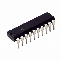
PIC16C770/P Microchip Technology, PIC16C770/P Datasheet - Page 17

PIC16C770/P
Manufacturer Part Number
PIC16C770/P
Description
IC MCU CMOS A/D 2K 20MHZ 20-DIP
Manufacturer
Microchip Technology
Series
PIC® 16Cr
Datasheets
1.PIC16C770-ISO.pdf
(220 pages)
2.PIC16C770-ISO.pdf
(6 pages)
3.PIC16C770-ISO.pdf
(8 pages)
Specifications of PIC16C770/P
Program Memory Type
OTP
Program Memory Size
3.5KB (2K x 14)
Package / Case
20-DIP (0.300", 7.62mm)
Core Processor
PIC
Core Size
8-Bit
Speed
20MHz
Connectivity
I²C, SPI
Peripherals
Brown-out Detect/Reset, POR, PWM, WDT
Number Of I /o
15
Ram Size
256 x 8
Voltage - Supply (vcc/vdd)
4 V ~ 5.5 V
Data Converters
A/D 6x12b
Oscillator Type
Internal
Operating Temperature
0°C ~ 70°C
Processor Series
PIC16C
Core
PIC
Data Bus Width
8 bit
Data Ram Size
256 B
Interface Type
I2C/SPI/SSP
Maximum Clock Frequency
20 MHz
Number Of Programmable I/os
16
Number Of Timers
3
Operating Supply Voltage
2.5 V to 5.5 V
Maximum Operating Temperature
+ 70 C
Mounting Style
Through Hole
3rd Party Development Tools
52715-96, 52716-328, 52717-734
Development Tools By Supplier
ICE2000
Minimum Operating Temperature
0 C
On-chip Adc
6-ch x 12-bit
Lead Free Status / RoHS Status
Lead free / RoHS Compliant
For Use With
DVA16XP200 - ADAPTER ICE 20DIP/SOIC/SSOPAC164028 - MODULE SKT PROMATEII 20SOIC/DIP
Eeprom Size
-
Lead Free Status / Rohs Status
Lead free / RoHS Compliant
- Current page: 17 of 220
- Download datasheet (4Mb)
2.2.2.2
The OPTION_REG register is a readable and writable
register, which contains various control bits to configure
the TMR0 prescaler/WDT postscaler (single assign-
able register known also as the prescaler), the External
INT Interrupt, TMR0 and the weak pull-ups on PORTB.
REGISTER 2-2:
2002 Microchip Technology Inc.
bit 7
bit 6
bit 5
bit 4
bit 3
bit 2-0
OPTION_REG REGISTER
OPTION REGISTER (OPTION_REG: 81h, 181h)
RBPU: PORTB Pull-up Enable bit
1 = PORTB weak pull-ups are disabled
0 = PORTB weak pull-ups are enabled by the WPUB register
INTEDG: Interrupt Edge Select bit
1 = Interrupt on rising edge of RB0/INT pin
0 = Interrupt on falling edge of RB0/INT pin
T0CS: TMR0 Clock Source Select bit
1 = Transition on RA4/T0CKI pin
0 = Internal instruction cycle clock (CLKOUT)
T0SE: TMR0 Source Edge Select bit
1 = Increment on high-to-low transition on RA4/T0CKI pin
0 = Increment on low-to-high transition on RA4/T0CKI pin
PSA: Prescaler Assignment bit
1 = Prescaler is assigned to the WDT
0 = Prescaler is assigned to the Timer0 module
PS<2:0>: Prescaler Rate Select bits
bit 7
Legend:
R = Readable bit
- n = Value at POR
R/W-1
RBPU
Note 1: Individual weak pull-up on RB pins can be enabled/disabled from the weak pull-up
Bit Value
PORTB Register (WPUB).
INTEDG
000
001
010
011
100
101
110
111
R/W-1
TMR0 Rate
1 : 2
1 : 4
1 : 8
1 : 16
1 : 32
1 : 64
1 : 128
1 : 256
R/W-1
T0CS
W = Writable bit
’1’ = Bit is set
(1)
WDT Rate
1 : 1
1 : 2
1 : 4
1 : 8
1 : 16
1 : 32
1 : 64
1 : 128
R/W-1
T0SE
Note:
PIC16C717/770/771
U = Unimplemented bit, read as ‘0’
’0’ = Bit is cleared
R/W-1
To achieve a 1:1 prescaler assignment for
the TMR0 register, assign the prescaler to
the Watchdog Timer.
PSA
R/W-1
PS2
x = Bit is unknown
R/W-1
PS1
DS41120B-page 15
R/W-1
PS0
bit 0
Related parts for PIC16C770/P
Image
Part Number
Description
Manufacturer
Datasheet
Request
R

Part Number:
Description:
IC, 8BIT MCU, PIC16C, 40MHZ, DIP-18
Manufacturer:
Microchip Technology
Datasheet:

Part Number:
Description:
IC, 8BIT MCU, PIC16C, 4MHZ, DIP-28
Manufacturer:
Microchip Technology
Datasheet:

Part Number:
Description:
IC, 8BIT MCU, PIC16C, 4MHZ, DIP-28
Manufacturer:
Microchip Technology
Datasheet:

Part Number:
Description:
IC, 8BIT MCU, PIC16C, 4MHZ, DIP-40
Manufacturer:
Microchip Technology
Datasheet:

Part Number:
Description:
SURFACE MOUNT POWER INDUCTORS
Manufacturer:
RCD [RCD COMPONENTS INC.]
Datasheet:

Part Number:
Description:
Manufacturer:
Microchip Technology Inc.
Datasheet:

Part Number:
Description:
Manufacturer:
Microchip Technology Inc.
Datasheet:

Part Number:
Description:
Manufacturer:
Microchip Technology Inc.
Datasheet:

Part Number:
Description:
Manufacturer:
Microchip Technology Inc.
Datasheet:

Part Number:
Description:
Manufacturer:
Microchip Technology Inc.
Datasheet:

Part Number:
Description:
Manufacturer:
Microchip Technology Inc.
Datasheet:


