PIC16C770/P Microchip Technology, PIC16C770/P Datasheet - Page 173
PIC16C770/P
Manufacturer Part Number
PIC16C770/P
Description
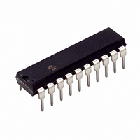
IC MCU CMOS A/D 2K 20MHZ 20-DIP
Manufacturer
Microchip Technology
Series
PIC® 16Cr
Datasheets
1.PIC16C770-ISO.pdf
(220 pages)
2.PIC16C770-ISO.pdf
(6 pages)
3.PIC16C770-ISO.pdf
(8 pages)
Specifications of PIC16C770/P
Program Memory Type
OTP
Program Memory Size
3.5KB (2K x 14)
Package / Case
20-DIP (0.300", 7.62mm)
Core Processor
PIC
Core Size
8-Bit
Speed
20MHz
Connectivity
I²C, SPI
Peripherals
Brown-out Detect/Reset, POR, PWM, WDT
Number Of I /o
15
Ram Size
256 x 8
Voltage - Supply (vcc/vdd)
4 V ~ 5.5 V
Data Converters
A/D 6x12b
Oscillator Type
Internal
Operating Temperature
0°C ~ 70°C
Processor Series
PIC16C
Core
PIC
Data Bus Width
8 bit
Data Ram Size
256 B
Interface Type
I2C/SPI/SSP
Maximum Clock Frequency
20 MHz
Number Of Programmable I/os
16
Number Of Timers
3
Operating Supply Voltage
2.5 V to 5.5 V
Maximum Operating Temperature
+ 70 C
Mounting Style
Through Hole
3rd Party Development Tools
52715-96, 52716-328, 52717-734
Development Tools By Supplier
ICE2000
Minimum Operating Temperature
0 C
On-chip Adc
6-ch x 12-bit
Lead Free Status / RoHS Status
Lead free / RoHS Compliant
For Use With
DVA16XP200 - ADAPTER ICE 20DIP/SOIC/SSOPAC164028 - MODULE SKT PROMATEII 20SOIC/DIP
Eeprom Size
-
Lead Free Status / Rohs Status
Lead free / RoHS Compliant


FIGURE 15-16:
TABLE 15-15: PIC16C717 AND PIC16LC717 A/D CONVERSION REQUIREMENT (NORMAL MODE)
130*
131*
132*
134*
Note 1: ADRES register may be read on the following T
Parameter
2002 Microchip Technology Inc.
*
†
No.
(3)
Note 1:
3: These numbers multiplied by 8 if V
2: See Section 11.6 for minimum conditions.
A/D DATA
SAMPLE
A/D CLK
These parameters are characterized but not tested.
Data in “Typ” column is at 5V, 25 C unless otherwise stated. These parameters are for design guidance only and are not
tested.
BSF ADCON0, GO
ADRES
ADIF
GO
T
T
T
T
If the A/D RC clock source is selected, a time of T
instruction to be executed.
AD
CNV
ACQ
Q4
GO
Sym
134
132
Characteristic
A/D clock period
Conversion time (not
including
acquisition time)
(Note 1)
Acquisition Time
Q4 to A/D clock start
PIC16C717 A/D CONVERSION TIMING (NORMAL MODE)
RH
or V
(Note 2)
9
RL
Min
1.6
3.0
3.0
2.0
—
5*
—
OLD_DATA
is selected as A/D reference.
CY
8
cycle.
SAMPLING STOPPED
131
T
7
11T
CY
Typ†
OSC
11.5
6.0
4.0
—
—
—
AD
is added before the A/D clock starts. This allows the SLEEP
/2
6
130
PIC16C717/770/771
3
Max
9.0
6.0
—
—
—
—
—
—
2
Units
T
—
AD
s
s
s
s
s
s
1
Tosc based, V
Tosc based, V
The minimum time is the amplifier
settling time. This may be used if
the “new” input voltage has not
changed by more than 1LSb (i.e.,
1mV @ 4.096V) from the last sam-
pled voltage (as stated on C
ADCS<1:0> = 11 (A/D RC mode)
1/2 T
0
CY
At V
At V
Conditions
NEW_DATA
DS41120B-page 171
REF
REF
DONE
DD
DD
full range
= 2.5V
= 5.0V
2.5V
HOLD
).
Related parts for PIC16C770/P
Image
Part Number
Description
Manufacturer
Datasheet
Request
R

Part Number:
Description:
IC, 8BIT MCU, PIC16C, 40MHZ, DIP-18
Manufacturer:
Microchip Technology
Datasheet:

Part Number:
Description:
IC, 8BIT MCU, PIC16C, 4MHZ, DIP-28
Manufacturer:
Microchip Technology
Datasheet:
Part Number:
Description:
IC, 8BIT MCU, PIC16C, 4MHZ, DIP-28
Manufacturer:
Microchip Technology
Datasheet:

Part Number:
Description:
IC, 8BIT MCU, PIC16C, 4MHZ, DIP-40
Manufacturer:
Microchip Technology
Datasheet:

Part Number:
Description:
SURFACE MOUNT POWER INDUCTORS
Manufacturer:
RCD [RCD COMPONENTS INC.]
Datasheet:

Part Number:
Description:
Manufacturer:
Microchip Technology Inc.
Datasheet:
Part Number:
Description:
Manufacturer:
Microchip Technology Inc.
Datasheet:
Part Number:
Description:
Manufacturer:
Microchip Technology Inc.
Datasheet:
Part Number:
Description:
Manufacturer:
Microchip Technology Inc.
Datasheet:
Part Number:
Description:
Manufacturer:
Microchip Technology Inc.
Datasheet:
Part Number:
Description:
Manufacturer:
Microchip Technology Inc.
Datasheet: