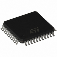
ST72F561J4T6 STMicroelectronics, ST72F561J4T6 Datasheet - Page 220

ST72F561J4T6
Manufacturer Part Number
ST72F561J4T6
Description
IC MCU 8BIT 16K FLASH 44-LQFP
Manufacturer
STMicroelectronics
Series
ST7r
Datasheet
1.ST72F561K6T6.pdf
(265 pages)
Specifications of ST72F561J4T6
Core Processor
ST7
Core Size
8-Bit
Speed
8MHz
Connectivity
CAN, LINSCI, SPI
Peripherals
LVD, POR, PWM, WDT
Number Of I /o
32
Program Memory Size
16KB (16K x 8)
Program Memory Type
FLASH
Ram Size
1K x 8
Voltage - Supply (vcc/vdd)
3.8 V ~ 5.5 V
Data Converters
A/D 16x10b
Oscillator Type
External
Operating Temperature
-40°C ~ 85°C
Package / Case
44-LQFP
Processor Series
ST72F5x
Core
ST7
Data Bus Width
8 bit
Data Ram Size
1 KB
Interface Type
CAN, SCI, SPI
Maximum Clock Frequency
8 MHz
Number Of Programmable I/os
48
Number Of Timers
3
Maximum Operating Temperature
+ 85 C
Mounting Style
SMD/SMT
Development Tools By Supplier
STX-RLINK
Minimum Operating Temperature
- 40 C
On-chip Adc
10 bit, 16 Channel
For Use With
497-8374 - BOARD DEVELOPMENT FOR ST72F561
Lead Free Status / RoHS Status
Lead free / RoHS Compliant
Eeprom Size
-
Lead Free Status / Rohs Status
Details
Available stocks
Company
Part Number
Manufacturer
Quantity
Price
Company:
Part Number:
ST72F561J4T6
Manufacturer:
COILCRAFT
Quantity:
4 000
Company:
Part Number:
ST72F561J4T6
Manufacturer:
STMicroelectronics
Quantity:
10 000
- Current page: 220 of 265
- Download datasheet (10Mb)
ST72561
12.2 ABSOLUTE MAXIMUM RATINGS
Stresses above those listed as “absolute maxi-
mum ratings” may cause permanent damage to
the device. This is a stress rating only and func-
tional operation of the device under these condi-
12.2.1 Voltage Characteristics
12.2.2 Current Characteristics
12.2.3 Thermal Characteristics
Notes:
1. Directly connecting the RESET and I/O pins to V
is generated or an unexpected change of the I/O configuration occurs (for example, due to a corrupted program counter).
To guarantee safe operation, this connection has to be done through a pull-up or pull-down resistor (typical: 4.7kΩ for
RESET, 10kΩ for I/Os). Unused I/O pins must be tied in the same way to V
2. I
respected, the injection current must be limited externally to the I
while a negative injection is induced by V
corresponding V
3. All power (V
4. Negative injection disturbs the analog performance of the device. See note in
page
5. When several inputs are submitted to a current injection, the maximum ΣI
and negative injected currents (instantaneous values). These results are based on characterization with ΣI
mum current injection on four I/O port pins of the device.
220/265
|ΔV
INJ(PIN)
245.
DDx
|V
I
V
ΣI
V
V
INJ(PIN)
V
SSA
Symbol
Symbol
Symbol
ESD(HBM)
DD
PP
INJ(PIN)
ESD(MM)
| and |ΔV
T
I
I
V
must never be exceeded. This is implicitly insured if V
VDD
VSS
I
STG
T
IO
- V
- V
- V
IN
J
2)4)
DD
SS
SS
SSx
2)
IN
) and ground (V
|
SSx
maximum must always be respected
|
Supply voltage
Programming Voltage
Input voltage on any pin
Variations between different digital power pins
Variations between digital and analog ground pins
Electro-static discharge voltage (Human Body Model)
Electro-static discharge voltage (Machine Model)
Total current into V
Total current out of V
Output current sunk by any standard I/O and control pin
Output current sunk by any high sink I/O pin
Output current source by any I/Os and control pin
Injected current on V
Injected current on RESET pin
Injected current on OSC1 and OSC2 pins
Injected current on PB3 (on Flash devices)
Injected current on any other pin
Total injected current (sum of all I/O and control pins)
Storage temperature range
Maximum junction temperature (see
SS
) lines must always be connected to the external supply.
IN
< V
DD
SS
PP
SS
power lines (source)
. For true open-drain pads, there is no positive injection current, and the
Ratings
Ratings
Ratings
1)2)
pin
ground lines (sink)
DD
or V
5)
SS
could damage the device if an unintentional internal reset
tions is not implied. Exposure to maximum rating
conditions for extended periods may affect device
reliability.
Section 13.2 "THERMAL
INJ(PIN)
IN
maximum is respected. If V
3)
3)
value. A positive injection is induced by V
DD
INJ(PIN)
or V
5)
SS
“10-BIT ADC CHARACTERISTICS” on
according to their reset configuration.
see
is the absolute sum of the positive
V
SS
Maximum value
Maximum value
Section 12.8.3 on page 233
- 0.3 to V
CHARACTERISTICS")
-65 to +150
Value
± 25
150
- 25
± 5
± 5
6.5
13
50
50
25
50
+5
IN
maximum cannot be
DD
+ 0.3
INJ(PIN)
Unit
Unit
Unit
mV
mA
IN
°C
V
>V
maxi-
DD
Related parts for ST72F561J4T6
Image
Part Number
Description
Manufacturer
Datasheet
Request
R

Part Number:
Description:
STMicroelectronics [RIPPLE-CARRY BINARY COUNTER/DIVIDERS]
Manufacturer:
STMicroelectronics
Datasheet:

Part Number:
Description:
STMicroelectronics [LIQUID-CRYSTAL DISPLAY DRIVERS]
Manufacturer:
STMicroelectronics
Datasheet:

Part Number:
Description:
BOARD EVAL FOR MEMS SENSORS
Manufacturer:
STMicroelectronics
Datasheet:

Part Number:
Description:
NPN TRANSISTOR POWER MODULE
Manufacturer:
STMicroelectronics
Datasheet:

Part Number:
Description:
TURBOSWITCH ULTRA-FAST HIGH VOLTAGE DIODE
Manufacturer:
STMicroelectronics
Datasheet:

Part Number:
Description:
Manufacturer:
STMicroelectronics
Datasheet:

Part Number:
Description:
DIODE / SCR MODULE
Manufacturer:
STMicroelectronics
Datasheet:

Part Number:
Description:
DIODE / SCR MODULE
Manufacturer:
STMicroelectronics
Datasheet:

Part Number:
Description:
Search -----> STE16N100
Manufacturer:
STMicroelectronics
Datasheet:

Part Number:
Description:
Search ---> STE53NA50
Manufacturer:
STMicroelectronics
Datasheet:

Part Number:
Description:
NPN Transistor Power Module
Manufacturer:
STMicroelectronics
Datasheet:

Part Number:
Description:
DIODE / SCR MODULE
Manufacturer:
STMicroelectronics
Datasheet:


