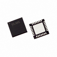
C8051F351-GMR Silicon Laboratories Inc, C8051F351-GMR Datasheet - Page 125

C8051F351-GMR
Manufacturer Part Number
C8051F351-GMR
Description
IC 8051 MCU 8K FLASH 28MLP
Manufacturer
Silicon Laboratories Inc
Series
C8051F35xr
Specifications of C8051F351-GMR
Core Processor
8051
Core Size
8-Bit
Speed
50MHz
Connectivity
SMBus (2-Wire/I²C), SPI, UART/USART
Peripherals
POR, PWM, Temp Sensor, WDT
Number Of I /o
17
Program Memory Size
8KB (8K x 8)
Program Memory Type
FLASH
Ram Size
768 x 8
Voltage - Supply (vcc/vdd)
2.7 V ~ 3.6 V
Data Converters
A/D 8x24b; D/A 2x8b
Oscillator Type
Internal
Operating Temperature
-40°C ~ 85°C
Package / Case
28-VQFN Exposed Pad, 28-HVQFN, 28-SQFN, 28-DHVQFN
Processor Series
C8051F3x
Core
8051
Data Bus Width
8 bit
Data Ram Size
768 B
Interface Type
I2C, SMBus, SPI, UART
Maximum Clock Frequency
50 MHz
Number Of Programmable I/os
17
Number Of Timers
4
Maximum Operating Temperature
+ 85 C
Mounting Style
SMD/SMT
3rd Party Development Tools
KSK-SL-TOOLSTICK, PK51, CA51, A51, ULINK2
Development Tools By Supplier
C8051F350DK
Minimum Operating Temperature
- 40 C
On-chip Adc
24 bit, 8 Channel
On-chip Dac
8 bit, 2 Channel
For Use With
336-1083 - DEV KIT FOR F350/351/352/353
Lead Free Status / RoHS Status
Lead free / RoHS Compliant
Eeprom Size
-
Lead Free Status / Rohs Status
Details
- Current page: 125 of 234
- Download datasheet (2Mb)
Bits7–2: UNUSED: Read = 000000b, Write = don’t care.
Bit1:
Bit0:
Bits7–0: FLKEY: Flash Lock and Key Register
R/W
Bit7
Bit7
—
R
PSEE: Program Store Erase Enable
Setting this bit (in combination with PSWE) allows an entire page of Flash program memory
to be erased. If this bit is logic 1 and Flash writes are enabled (PSWE is logic 1), a write to
Flash memory using the MOVX instruction will erase the entire page that contains the loca-
tion addressed by the MOVX instruction. The value of the data byte written does not matter.
0: Flash program memory erasure disabled.
1: Flash program memory erasure enabled.
PSWE: Program Store Write Enable
Setting this bit allows writing a byte of data to the Flash program memory using the MOVX
write instruction. The Flash location should be erased before writing data.
0: Writes to Flash program memory disabled.
1: Writes to Flash program memory enabled; the MOVX write instruction targets Flash
memory.
Write:
This register provides a lock and key function for Flash erasures and writes. Flash writes
and erases are enabled by writing 0xA5 followed by 0xF1 to the FLKEY register. Flash
writes and erases are automatically disabled after the next write or erase is complete. If any
writes to FLKEY are performed incorrectly, or if a Flash write or erase operation is attempted
while these operations are disabled, the Flash will be permanently locked from writes or era-
sures until the next device reset. If an application never writes to Flash, it can intentionally
lock the Flash by writing a non-0xA5 value to FLKEY from software.
Read:
When read, bits 1–0 indicate the current Flash lock state.
00: Flash is write/erase locked.
01: The first key code has been written (0xA5).
10: Flash is unlocked (writes/erases allowed).
11: Flash writes/erases disabled until the next reset.
SFR Definition 15.1. PSCTL: Program Store R/W Control
R/W
Bit6
Bit6
—
R
SFR Definition 15.2. FLKEY: Flash Lock and Key
R/W
Bit5
Bit5
—
R
R/W
Bit4
Bit4
—
R
Rev. 1.1
R/W
Bit3
Bit3
—
R
R/W
Bit2
Bit2
—
R
C8051F350/1/2/3
PSEE
R/W
R/W
Bit1
Bit1
SFR Address:
SFR Address:
PSWE
R/W
R/W
Bit0
Bit0
0x8F
0xB7
00000000
00000000
Reset Value
Reset Value
125
Related parts for C8051F351-GMR
Image
Part Number
Description
Manufacturer
Datasheet
Request
R
Part Number:
Description:
SMD/C°/SINGLE-ENDED OUTPUT SILICON OSCILLATOR
Manufacturer:
Silicon Laboratories Inc
Part Number:
Description:
Manufacturer:
Silicon Laboratories Inc
Datasheet:
Part Number:
Description:
N/A N/A/SI4010 AES KEYFOB DEMO WITH LCD RX
Manufacturer:
Silicon Laboratories Inc
Datasheet:
Part Number:
Description:
N/A N/A/SI4010 SIMPLIFIED KEY FOB DEMO WITH LED RX
Manufacturer:
Silicon Laboratories Inc
Datasheet:
Part Number:
Description:
N/A/-40 TO 85 OC/EZLINK MODULE; F930/4432 HIGH BAND (REV E/B1)
Manufacturer:
Silicon Laboratories Inc
Part Number:
Description:
EZLink Module; F930/4432 Low Band (rev e/B1)
Manufacturer:
Silicon Laboratories Inc
Part Number:
Description:
I°/4460 10 DBM RADIO TEST CARD 434 MHZ
Manufacturer:
Silicon Laboratories Inc
Part Number:
Description:
I°/4461 14 DBM RADIO TEST CARD 868 MHZ
Manufacturer:
Silicon Laboratories Inc
Part Number:
Description:
I°/4463 20 DBM RFSWITCH RADIO TEST CARD 460 MHZ
Manufacturer:
Silicon Laboratories Inc
Part Number:
Description:
I°/4463 20 DBM RADIO TEST CARD 868 MHZ
Manufacturer:
Silicon Laboratories Inc
Part Number:
Description:
I°/4463 27 DBM RADIO TEST CARD 868 MHZ
Manufacturer:
Silicon Laboratories Inc
Part Number:
Description:
I°/4463 SKYWORKS 30 DBM RADIO TEST CARD 915 MHZ
Manufacturer:
Silicon Laboratories Inc
Part Number:
Description:
N/A N/A/-40 TO 85 OC/4463 RFMD 30 DBM RADIO TEST CARD 915 MHZ
Manufacturer:
Silicon Laboratories Inc
Part Number:
Description:
I°/4463 20 DBM RADIO TEST CARD 169 MHZ
Manufacturer:
Silicon Laboratories Inc


