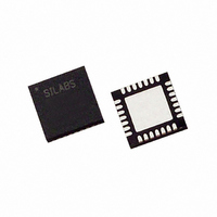
C8051F351-GMR Silicon Laboratories Inc, C8051F351-GMR Datasheet - Page 214

C8051F351-GMR
Manufacturer Part Number
C8051F351-GMR
Description
IC 8051 MCU 8K FLASH 28MLP
Manufacturer
Silicon Laboratories Inc
Series
C8051F35xr
Specifications of C8051F351-GMR
Core Processor
8051
Core Size
8-Bit
Speed
50MHz
Connectivity
SMBus (2-Wire/I²C), SPI, UART/USART
Peripherals
POR, PWM, Temp Sensor, WDT
Number Of I /o
17
Program Memory Size
8KB (8K x 8)
Program Memory Type
FLASH
Ram Size
768 x 8
Voltage - Supply (vcc/vdd)
2.7 V ~ 3.6 V
Data Converters
A/D 8x24b; D/A 2x8b
Oscillator Type
Internal
Operating Temperature
-40°C ~ 85°C
Package / Case
28-VQFN Exposed Pad, 28-HVQFN, 28-SQFN, 28-DHVQFN
Processor Series
C8051F3x
Core
8051
Data Bus Width
8 bit
Data Ram Size
768 B
Interface Type
I2C, SMBus, SPI, UART
Maximum Clock Frequency
50 MHz
Number Of Programmable I/os
17
Number Of Timers
4
Maximum Operating Temperature
+ 85 C
Mounting Style
SMD/SMT
3rd Party Development Tools
KSK-SL-TOOLSTICK, PK51, CA51, A51, ULINK2
Development Tools By Supplier
C8051F350DK
Minimum Operating Temperature
- 40 C
On-chip Adc
24 bit, 8 Channel
On-chip Dac
8 bit, 2 Channel
For Use With
336-1083 - DEV KIT FOR F350/351/352/353
Lead Free Status / RoHS Status
Lead free / RoHS Compliant
Eeprom Size
-
Lead Free Status / Rohs Status
Details
- Current page: 214 of 234
- Download datasheet (2Mb)
C8051F350/1/2/3
23.2.1. Edge-triggered Capture Mode
In this mode, a valid transition on the CEXn pin causes the PCA to capture the value of the PCA
counter/timer and load it into the corresponding module's 16-bit capture/compare register (PCA0CPLn and
PCA0CPHn). The CAPPn and CAPNn bits in the PCA0CPMn register are used to select the type of transi-
tion that triggers the capture: low-to-high transition (positive edge), high-to-low transition (negative edge),
or either transition (positive or negative edge). When a capture occurs, the Capture/Compare Flag (CCFn)
in PCA0CN is set to logic 1 and an interrupt request is generated if CCF interrupts are enabled. The CCFn
bit is not automatically cleared by hardware when the CPU vectors to the interrupt service routine, and
must be cleared by software. If both CAPPn and CAPNn bits are set to logic 1, then the state of the Port
pin associated with CEXn can be read directly to determine whether a rising-edge or falling-edge caused
the capture.
Note: The CEXn input signal must remain high or low for at least 2 system clock cycles to be recognized by
the hardware.
214
Port I/O
Crossbar
Figure 23.4. PCA Capture Mode Diagram
CEXn
W
P
M
1
6
n
x
PCA0CPMn
C
O
M
E
n
0
Rev. 1.1
C
A
P
P
n
C
A
P
N
n
0
1
M
A
T
n
x 0 0 x
O
G
T
n
W
P
M
n
C
C
E
F
n
0
1
C
F
C
R
PCA0CN
C
C
F
4
C
C
F
3
PCA
Timebase
C
C
F
2
C
C
F
1
PCA Interrupt
C
C
F
0
Capture
PCA0CPLn
PCA0L
PCA0CPHn
PCA0H
Related parts for C8051F351-GMR
Image
Part Number
Description
Manufacturer
Datasheet
Request
R
Part Number:
Description:
SMD/C°/SINGLE-ENDED OUTPUT SILICON OSCILLATOR
Manufacturer:
Silicon Laboratories Inc
Part Number:
Description:
Manufacturer:
Silicon Laboratories Inc
Datasheet:
Part Number:
Description:
N/A N/A/SI4010 AES KEYFOB DEMO WITH LCD RX
Manufacturer:
Silicon Laboratories Inc
Datasheet:
Part Number:
Description:
N/A N/A/SI4010 SIMPLIFIED KEY FOB DEMO WITH LED RX
Manufacturer:
Silicon Laboratories Inc
Datasheet:
Part Number:
Description:
N/A/-40 TO 85 OC/EZLINK MODULE; F930/4432 HIGH BAND (REV E/B1)
Manufacturer:
Silicon Laboratories Inc
Part Number:
Description:
EZLink Module; F930/4432 Low Band (rev e/B1)
Manufacturer:
Silicon Laboratories Inc
Part Number:
Description:
I°/4460 10 DBM RADIO TEST CARD 434 MHZ
Manufacturer:
Silicon Laboratories Inc
Part Number:
Description:
I°/4461 14 DBM RADIO TEST CARD 868 MHZ
Manufacturer:
Silicon Laboratories Inc
Part Number:
Description:
I°/4463 20 DBM RFSWITCH RADIO TEST CARD 460 MHZ
Manufacturer:
Silicon Laboratories Inc
Part Number:
Description:
I°/4463 20 DBM RADIO TEST CARD 868 MHZ
Manufacturer:
Silicon Laboratories Inc
Part Number:
Description:
I°/4463 27 DBM RADIO TEST CARD 868 MHZ
Manufacturer:
Silicon Laboratories Inc
Part Number:
Description:
I°/4463 SKYWORKS 30 DBM RADIO TEST CARD 915 MHZ
Manufacturer:
Silicon Laboratories Inc
Part Number:
Description:
N/A N/A/-40 TO 85 OC/4463 RFMD 30 DBM RADIO TEST CARD 915 MHZ
Manufacturer:
Silicon Laboratories Inc
Part Number:
Description:
I°/4463 20 DBM RADIO TEST CARD 169 MHZ
Manufacturer:
Silicon Laboratories Inc


