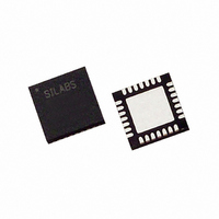
C8051F351-GMR Silicon Laboratories Inc, C8051F351-GMR Datasheet - Page 217

C8051F351-GMR
Manufacturer Part Number
C8051F351-GMR
Description
IC 8051 MCU 8K FLASH 28MLP
Manufacturer
Silicon Laboratories Inc
Series
C8051F35xr
Specifications of C8051F351-GMR
Core Processor
8051
Core Size
8-Bit
Speed
50MHz
Connectivity
SMBus (2-Wire/I²C), SPI, UART/USART
Peripherals
POR, PWM, Temp Sensor, WDT
Number Of I /o
17
Program Memory Size
8KB (8K x 8)
Program Memory Type
FLASH
Ram Size
768 x 8
Voltage - Supply (vcc/vdd)
2.7 V ~ 3.6 V
Data Converters
A/D 8x24b; D/A 2x8b
Oscillator Type
Internal
Operating Temperature
-40°C ~ 85°C
Package / Case
28-VQFN Exposed Pad, 28-HVQFN, 28-SQFN, 28-DHVQFN
Processor Series
C8051F3x
Core
8051
Data Bus Width
8 bit
Data Ram Size
768 B
Interface Type
I2C, SMBus, SPI, UART
Maximum Clock Frequency
50 MHz
Number Of Programmable I/os
17
Number Of Timers
4
Maximum Operating Temperature
+ 85 C
Mounting Style
SMD/SMT
3rd Party Development Tools
KSK-SL-TOOLSTICK, PK51, CA51, A51, ULINK2
Development Tools By Supplier
C8051F350DK
Minimum Operating Temperature
- 40 C
On-chip Adc
24 bit, 8 Channel
On-chip Dac
8 bit, 2 Channel
For Use With
336-1083 - DEV KIT FOR F350/351/352/353
Lead Free Status / RoHS Status
Lead free / RoHS Compliant
Eeprom Size
-
Lead Free Status / Rohs Status
Details
- Current page: 217 of 234
- Download datasheet (2Mb)
23.2.4. Frequency Output Mode
Frequency Output Mode produces a programmable-frequency square wave on the module’s associated
CEXn pin. The capture/compare module high byte holds the number of PCA clocks to count before the out-
put is toggled. The frequency of the square wave is then defined by Equation 23.1.
Where F
PCA0MD. The lower byte of the capture/compare module is compared to the PCA counter low byte; on a
match, CEXn is toggled and the offset held in the high byte is added to the matched value in PCA0CPLn.
Frequency Output Mode is enabled by setting the ECOMn, TOGn, and PWMn bits in the PCA0CPMn reg-
ister.
Note: A value of 0x00 in the PCA0CPHn register is equal to 256 for this equation.
PCA0CPLn
Write to
Reset
PCA0CPHn
PCA
Write to
is the frequency of the clock selected by the CPS2–0 bits in the PCA mode register,
0
ENB
ENB
1
Equation 23.1. Square Wave Frequency Output
W
P
M
1
6
n
x
Figure 23.7. PCA Frequency Output Mode
E
C
O
M
n
PCA0CPMn
C
A
P
P
n
0 0 0
C
A
P
N
n
M
A
T
n
O
G
T
n
W
P
M
n
E
C
C
F
n
x
PCA Timebase
F
CEXn
Enable
=
Comparator
PCA0CPLn
Rev. 1.1
---------------------------------------- -
2 PCA 0 CPHn
PCA0L
8-bit
×
F
PCA
match
Enable
Adder
8-bit Adder
Toggle
C8051F350/1/2/3
TOGn
0
1
CEXn
PCA0CPHn
Crossbar
Port I/O
217
Related parts for C8051F351-GMR
Image
Part Number
Description
Manufacturer
Datasheet
Request
R
Part Number:
Description:
SMD/C°/SINGLE-ENDED OUTPUT SILICON OSCILLATOR
Manufacturer:
Silicon Laboratories Inc
Part Number:
Description:
Manufacturer:
Silicon Laboratories Inc
Datasheet:
Part Number:
Description:
N/A N/A/SI4010 AES KEYFOB DEMO WITH LCD RX
Manufacturer:
Silicon Laboratories Inc
Datasheet:
Part Number:
Description:
N/A N/A/SI4010 SIMPLIFIED KEY FOB DEMO WITH LED RX
Manufacturer:
Silicon Laboratories Inc
Datasheet:
Part Number:
Description:
N/A/-40 TO 85 OC/EZLINK MODULE; F930/4432 HIGH BAND (REV E/B1)
Manufacturer:
Silicon Laboratories Inc
Part Number:
Description:
EZLink Module; F930/4432 Low Band (rev e/B1)
Manufacturer:
Silicon Laboratories Inc
Part Number:
Description:
I°/4460 10 DBM RADIO TEST CARD 434 MHZ
Manufacturer:
Silicon Laboratories Inc
Part Number:
Description:
I°/4461 14 DBM RADIO TEST CARD 868 MHZ
Manufacturer:
Silicon Laboratories Inc
Part Number:
Description:
I°/4463 20 DBM RFSWITCH RADIO TEST CARD 460 MHZ
Manufacturer:
Silicon Laboratories Inc
Part Number:
Description:
I°/4463 20 DBM RADIO TEST CARD 868 MHZ
Manufacturer:
Silicon Laboratories Inc
Part Number:
Description:
I°/4463 27 DBM RADIO TEST CARD 868 MHZ
Manufacturer:
Silicon Laboratories Inc
Part Number:
Description:
I°/4463 SKYWORKS 30 DBM RADIO TEST CARD 915 MHZ
Manufacturer:
Silicon Laboratories Inc
Part Number:
Description:
N/A N/A/-40 TO 85 OC/4463 RFMD 30 DBM RADIO TEST CARD 915 MHZ
Manufacturer:
Silicon Laboratories Inc
Part Number:
Description:
I°/4463 20 DBM RADIO TEST CARD 169 MHZ
Manufacturer:
Silicon Laboratories Inc


