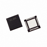
C8051F351-GMR Silicon Laboratories Inc, C8051F351-GMR Datasheet - Page 45

C8051F351-GMR
Manufacturer Part Number
C8051F351-GMR
Description
IC 8051 MCU 8K FLASH 28MLP
Manufacturer
Silicon Laboratories Inc
Series
C8051F35xr
Specifications of C8051F351-GMR
Core Processor
8051
Core Size
8-Bit
Speed
50MHz
Connectivity
SMBus (2-Wire/I²C), SPI, UART/USART
Peripherals
POR, PWM, Temp Sensor, WDT
Number Of I /o
17
Program Memory Size
8KB (8K x 8)
Program Memory Type
FLASH
Ram Size
768 x 8
Voltage - Supply (vcc/vdd)
2.7 V ~ 3.6 V
Data Converters
A/D 8x24b; D/A 2x8b
Oscillator Type
Internal
Operating Temperature
-40°C ~ 85°C
Package / Case
28-VQFN Exposed Pad, 28-HVQFN, 28-SQFN, 28-DHVQFN
Processor Series
C8051F3x
Core
8051
Data Bus Width
8 bit
Data Ram Size
768 B
Interface Type
I2C, SMBus, SPI, UART
Maximum Clock Frequency
50 MHz
Number Of Programmable I/os
17
Number Of Timers
4
Maximum Operating Temperature
+ 85 C
Mounting Style
SMD/SMT
3rd Party Development Tools
KSK-SL-TOOLSTICK, PK51, CA51, A51, ULINK2
Development Tools By Supplier
C8051F350DK
Minimum Operating Temperature
- 40 C
On-chip Adc
24 bit, 8 Channel
On-chip Dac
8 bit, 2 Channel
For Use With
336-1083 - DEV KIT FOR F350/351/352/353
Lead Free Status / RoHS Status
Lead free / RoHS Compliant
Eeprom Size
-
Lead Free Status / Rohs Status
Details
- Current page: 45 of 234
- Download datasheet (2Mb)
The offset calibration value adjusts the zero point of the ADC’s transfer function. It is stored as a two’s
complement, 24-bit number. An offset calibration which results in a full-scale positive (0x7FFFFF) or full-
scale negative (0x800000) result will cause an ADC error condition.
The Offset Calibration results are stored in registers ADC0COH, ADC0COM, and ADC0COL. The weight-
ing of the bits in the offset register (in LSBs) are shown below:
The gain calibration value adjusts the slope of the ADC’s transfer function. The gain calibration regsiter
can range from 0 to 2 – 2
ADC error condition.
The Gain Calibration results are stored in registers ADC0CGH, ADC0CGM, and ADC0CGL, as follows:
Example Decoding for Gain Register setting of 0x940000 (10010100 00000000 00000000b):
Slope Adjustment = 2
MSB 22
MSB 22
MSB 22
–
–2
2
2
0
15
23
2
2
2
14
–1
22
2
2
2
21
21
21
13
–2
21
ADC0COH
ADC0COH
ADC0CGH
2
2
2
20
20
20
12
–3
20
2
2
2
19
19
19
Figure 5.3. ADC0 Offset Calibration Register Coding
11
–4
19
Figure 5.4. ADC0 Gain Calibration Register Coding
0
2
2
2
18
18
18
+ 2
–5
18
10
–23
–3
2
2
17
17
17
2
17
–6
+ 2
9
. A gain calibration which results in either of these extremes will cause an
2
2
–5
16
16
16
2
16
–7
8
= 1.0 + 0.125 + 0.03125 = 1.15625
2
2
15
15
15
2
15
–8
7
24-bit ADC (C8051F350/1)
16-bit ADC (C8051F352/3)
2
2
14
14
14
2
14
–9
6
2
2
13
13
13
2
–10
13
5
ADC0COM
ADC0CGM
ADC0COM
2
Rev. 1.1
2
12
12
12
2
–11
12
4
2
2
11
11
11
2
–12
11
3
2
2
10
10
10
2
–13
10
2
2
2
2
9
–14
9
9
9
1
2
2
8
2
–15
8
8
8
0
C8051F350/1/2/3
2
2
2
7
–16
7
7
–1
7
2
2
2
6
–17
6
6
6
–2
2
2
2
5
–18
5
5
5
–3
ADC0COL
ADC0COL
ADC0CGL
2
2
2
4
–19
4
4
4
–4
2
2
2
3
–20
3
3
3
–5
2
2
2
2
–21
2
2
2
–6
2
2
2
1
–22
1
1
1
–7
LSB
LSB
2
LSB
2
2
–23
0
–8
45
Related parts for C8051F351-GMR
Image
Part Number
Description
Manufacturer
Datasheet
Request
R
Part Number:
Description:
SMD/C°/SINGLE-ENDED OUTPUT SILICON OSCILLATOR
Manufacturer:
Silicon Laboratories Inc
Part Number:
Description:
Manufacturer:
Silicon Laboratories Inc
Datasheet:
Part Number:
Description:
N/A N/A/SI4010 AES KEYFOB DEMO WITH LCD RX
Manufacturer:
Silicon Laboratories Inc
Datasheet:
Part Number:
Description:
N/A N/A/SI4010 SIMPLIFIED KEY FOB DEMO WITH LED RX
Manufacturer:
Silicon Laboratories Inc
Datasheet:
Part Number:
Description:
N/A/-40 TO 85 OC/EZLINK MODULE; F930/4432 HIGH BAND (REV E/B1)
Manufacturer:
Silicon Laboratories Inc
Part Number:
Description:
EZLink Module; F930/4432 Low Band (rev e/B1)
Manufacturer:
Silicon Laboratories Inc
Part Number:
Description:
I°/4460 10 DBM RADIO TEST CARD 434 MHZ
Manufacturer:
Silicon Laboratories Inc
Part Number:
Description:
I°/4461 14 DBM RADIO TEST CARD 868 MHZ
Manufacturer:
Silicon Laboratories Inc
Part Number:
Description:
I°/4463 20 DBM RFSWITCH RADIO TEST CARD 460 MHZ
Manufacturer:
Silicon Laboratories Inc
Part Number:
Description:
I°/4463 20 DBM RADIO TEST CARD 868 MHZ
Manufacturer:
Silicon Laboratories Inc
Part Number:
Description:
I°/4463 27 DBM RADIO TEST CARD 868 MHZ
Manufacturer:
Silicon Laboratories Inc
Part Number:
Description:
I°/4463 SKYWORKS 30 DBM RADIO TEST CARD 915 MHZ
Manufacturer:
Silicon Laboratories Inc
Part Number:
Description:
N/A N/A/-40 TO 85 OC/4463 RFMD 30 DBM RADIO TEST CARD 915 MHZ
Manufacturer:
Silicon Laboratories Inc
Part Number:
Description:
I°/4463 20 DBM RADIO TEST CARD 169 MHZ
Manufacturer:
Silicon Laboratories Inc


