MC9S08GT60ACFBE Freescale Semiconductor, MC9S08GT60ACFBE Datasheet - Page 124
MC9S08GT60ACFBE
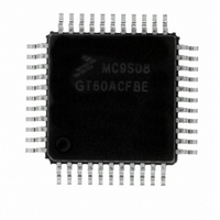
Manufacturer Part Number
MC9S08GT60ACFBE
Description
IC MCU 60K FLASH 4K RAM 44-QFP
Manufacturer
Freescale Semiconductor
Series
HCS08r
Datasheet
1.MC9S08GT60ACFDER.pdf
(302 pages)
Specifications of MC9S08GT60ACFBE
Core Processor
HCS08
Core Size
8-Bit
Speed
40MHz
Connectivity
I²C, SCI, SPI
Peripherals
LVD, POR, PWM, WDT
Number Of I /o
36
Program Memory Size
60KB (60K x 8)
Program Memory Type
FLASH
Ram Size
4K x 8
Voltage - Supply (vcc/vdd)
1.8 V ~ 3.6 V
Data Converters
A/D 8x10b
Oscillator Type
Internal
Operating Temperature
-40°C ~ 85°C
Package / Case
44-QFP
Cpu Family
HCS08
Device Core Size
8b
Frequency (max)
40MHz
Interface Type
I2C/SCI/SPI
Total Internal Ram Size
4KB
# I/os (max)
36
Number Of Timers - General Purpose
4
Operating Supply Voltage (typ)
2.5/3.3V
Operating Supply Voltage (max)
3.6V
Operating Supply Voltage (min)
1.8/2.08V
On-chip Adc
8-chx10-bit
Instruction Set Architecture
CISC
Operating Temp Range
-40C to 85C
Operating Temperature Classification
Industrial
Mounting
Surface Mount
Pin Count
44
Package Type
PQFP
Processor Series
S08GT
Core
HCS08
Data Bus Width
8 bit
Data Ram Size
4 KB
Maximum Clock Frequency
20 MHz
Number Of Programmable I/os
39
Number Of Timers
2
Operating Supply Voltage
0 V to 1.8 V
Maximum Operating Temperature
+ 85 C
Mounting Style
SMD/SMT
3rd Party Development Tools
EWS08
Development Tools By Supplier
M68EVB908GB60E, M68DEMO908GB60E
Minimum Operating Temperature
- 40 C
For Use With
M68DEMO908GB60E - BOARD DEMO MC9S08GB60M68EVB908GB60E - BOARD EVAL FOR MC9S08GB60
Lead Free Status / RoHS Status
Lead free / RoHS Compliant
Eeprom Size
-
Lead Free Status / Rohs Status
Compliant
Available stocks
Company
Part Number
Manufacturer
Quantity
Price
Company:

Part Number:
MC9S08GT60ACFBE
Manufacturer:
Freescale Semiconductor
Quantity:
10 000
Part Number:
MC9S08GT60ACFBE
Manufacturer:
FREESCALE深圳进口
Quantity:
20 000
Company:
Part Number:
MC9S08GT60ACFBER
Manufacturer:
Freescale Semiconductor
Quantity:
10 000


Internal Clock Generator (S08ICGV2)
7.5.1
124
OSCSTEN
Reset
RANGE
LOCD
REFS
CLKS
Field
HGO
4:3
7
6
5
2
1
W
R
ICG Control Register 1 (ICGC1)
HGO
High Gain Oscillator Select — The HGO bit is used to select between low-power operation and high-amplitude
operation.
0 Oscillator configured for low power operation.
1 Oscillator configured for high amplitude operation.
Frequency Range Select — The RANGE bit controls the oscillator, reference divider, and FLL loop prescaler
multiplication factor (P). It selects one of two reference frequency ranges for the ICG. The RANGE bit is
write-once after a reset. The RANGE bit only has an effect in FLL engaged external and FLL bypassed external
modes.
0 Oscillator configured for low frequency range. FLL loop prescale factor P is 64.
1 Oscillator configured for high frequency range. FLL loop prescale factor P is 1.
External Reference Select — The REFS bit controls the external reference clock source for ICGERCLK. The
REFS bit is write-once after a reset.
0 External clock requested.
1 Oscillator using crystal or resonator requested.
Clock Mode Select — The CLKS bits control the clock mode. If FLL bypassed external is requested, it will not
be selected until ERCS = 1. If the ICG enters off mode, the CLKS bits will remain unchanged. Writes to the CLKS
bits will not take effect if a previous write is not complete.
The CLKS bits are writable at any time, unless the first write after a reset was CLKS = 0X, the CLKS bits cannot
be written to 1X until after the next reset (because the EXTAL pin was not reserved).
00 Self-clocked
01 FLL engaged, internal reference
10 FLL bypassed, external reference
11 FLL engaged, external reference
Enable Oscillator in Off Mode — The OSCTEN bit controls whether or not the oscillator circuit remains enabled
when the ICG enters off mode.
0 Oscillator disabled when ICG is in off mode unless ENABLE is high, CLKS = 10, and REFST = 1.
1 Oscillator enabled when ICG is in off mode, CLKS = 1X and REFST = 1.
Loss of Clock Disable
0 Loss of clock detection enabled.
1 Loss of clock detection disabled.
0
7
= Unimplemented or Reserved
RANGE
1
6
Figure 7-12. ICG Control Register 1 (ICGC1)
Table 7-6. ICGC1 Field Descriptions
REFS
MC9S08GB60A Data Sheet, Rev. 2
0
5
0
4
Description
CLKS
3
0
OSCSTEN
1
2
Freescale Semiconductor
LOCD
0
1
0
0
0
Related parts for MC9S08GT60ACFBE
Image
Part Number
Description
Manufacturer
Datasheet
Request
R

Part Number:
Description:
Manufacturer:
Freescale Semiconductor, Inc
Datasheet:
Part Number:
Description:
Manufacturer:
Freescale Semiconductor, Inc
Datasheet:
Part Number:
Description:
Manufacturer:
Freescale Semiconductor, Inc
Datasheet:
Part Number:
Description:
Manufacturer:
Freescale Semiconductor, Inc
Datasheet:
Part Number:
Description:
Manufacturer:
Freescale Semiconductor, Inc
Datasheet:
Part Number:
Description:
Manufacturer:
Freescale Semiconductor, Inc
Datasheet:
Part Number:
Description:
Manufacturer:
Freescale Semiconductor, Inc
Datasheet:
Part Number:
Description:
Manufacturer:
Freescale Semiconductor, Inc
Datasheet:
Part Number:
Description:
Manufacturer:
Freescale Semiconductor, Inc
Datasheet:
Part Number:
Description:
Manufacturer:
Freescale Semiconductor, Inc
Datasheet:
Part Number:
Description:
Manufacturer:
Freescale Semiconductor, Inc
Datasheet:
Part Number:
Description:
Manufacturer:
Freescale Semiconductor, Inc
Datasheet:
Part Number:
Description:
Manufacturer:
Freescale Semiconductor, Inc
Datasheet:
Part Number:
Description:
Manufacturer:
Freescale Semiconductor, Inc
Datasheet:
Part Number:
Description:
Manufacturer:
Freescale Semiconductor, Inc
Datasheet: