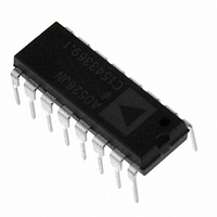
AD526JNZ Analog Devices Inc, AD526JNZ Datasheet - Page 11

AD526JNZ
Manufacturer Part Number
AD526JNZ
Description
IC AMP PGA 10MA 16DIP
Manufacturer
Analog Devices Inc
Type
Programmable Gain Amplifierr
Datasheet
1.AD526JNZ.pdf
(14 pages)
Specifications of AD526JNZ
Amplifier Type
Programmable Gain
Number Of Circuits
1
Slew Rate
24 V/µs
-3db Bandwidth
4MHz
Current - Input Bias
50pA
Voltage - Input Offset
400µV
Current - Supply
10mA
Current - Output / Channel
10mA
Voltage - Supply, Single/dual (±)
±4.5 V ~ 16.5 V
Operating Temperature
0°C ~ 70°C
Mounting Type
Through Hole
Package / Case
16-DIP (0.300", 7.62mm)
No. Of Amplifiers
1
Bandwidth
350kHz
No. Of Channels
1
Supply Voltage Range
± 4.5V To ± 16V
Amplifier Case Style
DIP
No. Of Pins
16
Operating Temperature Range
0°C To +70°C
Number Of Channels
1
Number Of Elements
1
Power Supply Requirement
Dual
Input Offset Voltage
1.5@±15VmV
Single Supply Voltage (typ)
Not RequiredV
Dual Supply Voltage (typ)
±5/±9/±12/±15V
Rail/rail I/o Type
No
Single Supply Voltage (min)
Not RequiredV
Single Supply Voltage (max)
Not RequiredV
Dual Supply Voltage (min)
±4.5V
Dual Supply Voltage (max)
±16.5V
Operating Temp Range
0C to 70C
Operating Temperature Classification
Commercial
Mounting
Through Hole
Pin Count
16
Package Type
PDIP
Lead Free Status / RoHS Status
Lead free / RoHS Compliant
Output Type
-
Gain Bandwidth Product
-
Lead Free Status / Rohs Status
Compliant
Available stocks
Company
Part Number
Manufacturer
Quantity
Price
REV. D
OFFSET NULLING
Input voltage offset nulling of the AD526 is best accomplished
at a gain of 16, since the referred-to-input (RTI) offset is ampli-
fied the most at this gain and therefore is most easily trimmed.
The resulting trimmed value of RTI voltage offset typically
varies less than 3 V across all gain ranges.
Note that the low input current of the AD526 minimizes RTI
voltage offsets due to source resistance.
OUTPUT CURRENT BOOSTER
The AD526 is rated for a full 10 V output voltage swing into
2 k . In some applications, the need exists to drive more cur-
rent into heavier loads. As shown in Figure 40, a high current
booster may be connected “inside the loop” of the SPGA to
provide the required current boost without significantly degrad-
ing overall performance. Nonlinearities, offset and gain inaccu-
racies of the buffer are minimized by the loop gain of the
AD526 output amplifier.
V
IN
V
IN
16
A1
1
AD526
16
LOGIC AND LATCHES
A0
15
2
16
A1
1
Figure 39. Offset Voltage Null Circuit
Figure 40. Current Output Boosting
GAIN NETWORK
AD526
8
16
14
CS CLK
LOGIC AND LATCHES
3
A0
15
2
4
GAIN NETWORK
20k
8
13
4
14
CS CLK
3
2
4
12
A2
5
13
1
4
2
11
B
6
12
A2
5
1
+
–
–V
+V
10
7
11
B
0.1 F
0.1 F
S
6
S
–
+
+V
–V
9
8
10
7
S
S
OUT
FORCE
OUT
SENSE
9
8
0.1 F
0.1 F
OUT
FORCE
OUT
SENSE
HOS-100
0.01 F
0.01 F
V
OUT
R
L
–11–
CASCADED OPERATION
A cascade of two AD526s can be used to achieve binarily
weighted gains from 1 to 256. If gains from 1 to 128 are needed,
no additional components are required. This is accomplished by
using the B pin as shown in Figure 38. When the B pin is low,
the AD526 is held in a unity gain stage independent of the other
gain code values.
OFFSET NULLING WITH A D/A CONVERTER
Figure 41 shows the AD526 with offset nulling accomplished
with an 8-bit D/A converter (AD7524) circuit instead of the
potentiometer shown in Figure 39. The calibration procedure is
the same as before except that instead of adjusting the potenti-
ometer, the D/A converter corrects for the offset error. This
calibration circuit has a number of benefits in addition to elimi-
nating the trimpot. The most significant benefit is that calibra-
tion can be under the control of a microprocessor and therefore
can be implemented as part of an autocalibration scheme. Sec-
ondly, dip switches or RAM can be used to hold the 8-bit word
after its value has been determined. In Figure 42 the offset null
sensitivity, at a gain of 16, is 80 V per LSB of adjustment,
which guarantees dc accuracy to the 16-bit performance level.
MSB
LSB
WR
CS
+V
S
Figure 41. Offset Nulling Using a DAC
AD7524
V
REF
V
AD581 OR
IN
AD587
GND
+10V
16
A1
1
AD526
16
LOGIC AND LATCHES
15
A0
2
OUT 2
3.3M
GAIN NETWORK
1k
OUT 1
8
14
CS CLK
3
4
ALL BYPASS CAPACITORS ARE 0.1 F
13
4
10 F
7.5M
2
12
A2
5
1
AD548
–
+
11
B
6
+V
–V
0.01 F
S
+
S
–
0.01 F
+V
–V
10
7
S
S
9
8
AD526
0.1 F
0.1 F
OUT
FORCE
OUT
SENSE
V
OUT


