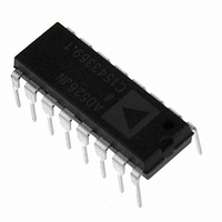
AD526JNZ Analog Devices Inc, AD526JNZ Datasheet - Page 3

AD526JNZ
Manufacturer Part Number
AD526JNZ
Description
IC AMP PGA 10MA 16DIP
Manufacturer
Analog Devices Inc
Type
Programmable Gain Amplifierr
Datasheet
1.AD526JNZ.pdf
(14 pages)
Specifications of AD526JNZ
Amplifier Type
Programmable Gain
Number Of Circuits
1
Slew Rate
24 V/µs
-3db Bandwidth
4MHz
Current - Input Bias
50pA
Voltage - Input Offset
400µV
Current - Supply
10mA
Current - Output / Channel
10mA
Voltage - Supply, Single/dual (±)
±4.5 V ~ 16.5 V
Operating Temperature
0°C ~ 70°C
Mounting Type
Through Hole
Package / Case
16-DIP (0.300", 7.62mm)
No. Of Amplifiers
1
Bandwidth
350kHz
No. Of Channels
1
Supply Voltage Range
± 4.5V To ± 16V
Amplifier Case Style
DIP
No. Of Pins
16
Operating Temperature Range
0°C To +70°C
Number Of Channels
1
Number Of Elements
1
Power Supply Requirement
Dual
Input Offset Voltage
1.5@±15VmV
Single Supply Voltage (typ)
Not RequiredV
Dual Supply Voltage (typ)
±5/±9/±12/±15V
Rail/rail I/o Type
No
Single Supply Voltage (min)
Not RequiredV
Single Supply Voltage (max)
Not RequiredV
Dual Supply Voltage (min)
±4.5V
Dual Supply Voltage (max)
±16.5V
Operating Temp Range
0C to 70C
Operating Temperature Classification
Commercial
Mounting
Through Hole
Pin Count
16
Package Type
PDIP
Lead Free Status / RoHS Status
Lead free / RoHS Compliant
Output Type
-
Gain Bandwidth Product
-
Lead Free Status / Rohs Status
Compliant
Available stocks
Company
Part Number
Manufacturer
Quantity
Price
REV. D
Model
NOISE, ALL GAINS
DYNAMIC RESPONSE
DIGITAL INPUTS
TIMING
TEMPERATURE RANGE
POWER SUPPLY
PACKAGE OPTIONS
NOTES
1
Specifications subject to change without notice.
Specifications shown in boldface are tested on all production units at final electrical test. All min and max specifications are guaranteed, although only those shown in
boldface are tested on all production units.
Refer to Figure 25 for definitions. FSR = Full Scale Range = 20 V. RTI = Referred to Input.
Voltage Noise, RTI
Voltage Noise Density, RTI
–3 dB Bandwidth (Small Signal)
Signal Settling Time to 0.01%
Full Power Bandwidth
Slew Rate
(T
(V
Specified Performance
Storage
Operating Range
Positive Supply Current
Negative Supply Current
Plastic (N-16)
Ceramic DIP (D-16)
0.1 Hz to 10 Hz
f = 10 Hz
f = 100 Hz
f = 1 kHz
f = 10 kHz
G = 1
G = 2
G = 4
G = 8
G = 16
( V
G = 1, 2, 4
G = 8, 16
G = 1, 2, 4
G = 8, 16
MIN
Input Current (V
Logic “1”
Logic “0”
L
A0, A1, A2
B
= 0.2 V, V
G = 1
G = 2
G = 4
G = 8
G = 16
T
T
T
T
T
T
OUT
to T
1
C
S
H
C
S
H
= 10 V)
MAX
H
)
= 3.7 V)
H
= 5 V)
Min
4
18
60
2
0
50
30
30
50
40
10
0
–65
4.5
AD526JN
AD526J
Typ
3
70
60
30
25
4.0
2.0
1.5
0.65
0.35
2.1
2.5
2.7
3.6
4.1
0.10
0.35
6
24
100
10
10
Max
4
5
5
7
7
140
6
0.8
+70
+125
14
13
16.5
Min
4
18
60
2
0
50
30
30
50
40
10
–65
–40
4.5
AD526AD
AD526A
–3–
Typ
3
70
60
30
25
4.0
2.0
1.5
0.65
0.35
2.1
2.5
2.7
3.6
4.1
0.10
0.35
6
24
100
10
10
Max
4
5
5
7
7
140
6
0.8
+150
14
13
+85
16.5
Min
4
18
60
2
0
50
30
30
50
40
10
–40/–55
–65
AD526BD AD526SD
4.5
AD526B/S
Typ
3
70
60
30
25
4.0
2.0
1.5
0.65
0.35
2.1
2.5
2.7
3.6
4.1
0.10
0.35
6
24
100
10
10
AD526SD/883B
Max
4
5
5
7
7
140
6
0.8
+85/+125 –40
+150
14
13
16.5
Min
4
18
60
2
0
50
30
30
50
40
30
–65
4.5
AD526C
Typ
3
70
60
30
35
4.0
2.0
1.5
0.65
0.35
2.1
2.5
2.7
3.6
4.1
0.10
0.35
6
24
100
10
10
AD526CD
Max
4
5
5
7
7
140
6
0.8
+85
+150
14
13
16.5 V
AD526
Units
nV Hz
nV Hz
nV Hz
nV Hz
MHz
MHz
MHz
MHz
MHz
MHz
MHz
V/ s
V/ s
V
V
ns
ns
ns
ns
ns
ns
mA
mA
C
C
V p-p
s
s
s
s
s
A


