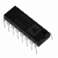
AD526JNZ Analog Devices Inc, AD526JNZ Datasheet - Page 6

AD526JNZ
Manufacturer Part Number
AD526JNZ
Description
IC AMP PGA 10MA 16DIP
Manufacturer
Analog Devices Inc
Type
Programmable Gain Amplifierr
Datasheet
1.AD526JNZ.pdf
(14 pages)
Specifications of AD526JNZ
Amplifier Type
Programmable Gain
Number Of Circuits
1
Slew Rate
24 V/µs
-3db Bandwidth
4MHz
Current - Input Bias
50pA
Voltage - Input Offset
400µV
Current - Supply
10mA
Current - Output / Channel
10mA
Voltage - Supply, Single/dual (±)
±4.5 V ~ 16.5 V
Operating Temperature
0°C ~ 70°C
Mounting Type
Through Hole
Package / Case
16-DIP (0.300", 7.62mm)
No. Of Amplifiers
1
Bandwidth
350kHz
No. Of Channels
1
Supply Voltage Range
± 4.5V To ± 16V
Amplifier Case Style
DIP
No. Of Pins
16
Operating Temperature Range
0°C To +70°C
Number Of Channels
1
Number Of Elements
1
Power Supply Requirement
Dual
Input Offset Voltage
1.5@±15VmV
Single Supply Voltage (typ)
Not RequiredV
Dual Supply Voltage (typ)
±5/±9/±12/±15V
Rail/rail I/o Type
No
Single Supply Voltage (min)
Not RequiredV
Single Supply Voltage (max)
Not RequiredV
Dual Supply Voltage (min)
±4.5V
Dual Supply Voltage (max)
±16.5V
Operating Temp Range
0C to 70C
Operating Temperature Classification
Commercial
Mounting
Through Hole
Pin Count
16
Package Type
PDIP
Lead Free Status / RoHS Status
Lead free / RoHS Compliant
Output Type
-
Gain Bandwidth Product
-
Lead Free Status / Rohs Status
Compliant
Available stocks
Company
Part Number
Manufacturer
Quantity
Price
AD526
**Scope Traces are: Top: Output Transition; Middle: Output Settling; Bottom: Digital Input.
Figure 19. Large Signal Pulse
Response and Settling Time,* G = 8
*For Settling Time Traces, 0.01% = 1/2 Vertical Division
Figure 25. Output Impedance vs.
Frequency
100
Figure 22. Small Signal Pulse
Response, Gain = 16
10
1
10k
G = 4, 16
FREQUENCY – Hz
100k
G = 1
1M
G = 2, 8
10M
Figure 23. Total Harmonic Distortion
vs. Frequency Gain = 16
Time,** Gain Change: 1 to 2
–100
Figure 26. Gain Change Settling
–60
–70
–80
–90
Figure 20. Small Signal Pulse
Response, G = 8
10
100
FREQUENCY – Hz
–6–
1k
10k
100k
Figure 21. Large Signal Pulse
Response and Settling Time,* G = 16
Time,** Gain Change 1 to 4
–10
Figure 27. Gain Change Settling
10
–5
Figure 24. Phase Distortion vs.
Frequency, Gain = 16
5
0
10
100
FREQUENCY – Hz
1k
10k
REV. D
100k


