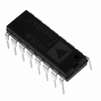
AD526JNZ Analog Devices Inc, AD526JNZ Datasheet - Page 13

AD526JNZ
Manufacturer Part Number
AD526JNZ
Description
IC AMP PGA 10MA 16DIP
Manufacturer
Analog Devices Inc
Type
Programmable Gain Amplifierr
Datasheet
1.AD526JNZ.pdf
(14 pages)
Specifications of AD526JNZ
Amplifier Type
Programmable Gain
Number Of Circuits
1
Slew Rate
24 V/µs
-3db Bandwidth
4MHz
Current - Input Bias
50pA
Voltage - Input Offset
400µV
Current - Supply
10mA
Current - Output / Channel
10mA
Voltage - Supply, Single/dual (±)
±4.5 V ~ 16.5 V
Operating Temperature
0°C ~ 70°C
Mounting Type
Through Hole
Package / Case
16-DIP (0.300", 7.62mm)
No. Of Amplifiers
1
Bandwidth
350kHz
No. Of Channels
1
Supply Voltage Range
± 4.5V To ± 16V
Amplifier Case Style
DIP
No. Of Pins
16
Operating Temperature Range
0°C To +70°C
Number Of Channels
1
Number Of Elements
1
Power Supply Requirement
Dual
Input Offset Voltage
1.5@±15VmV
Single Supply Voltage (typ)
Not RequiredV
Dual Supply Voltage (typ)
±5/±9/±12/±15V
Rail/rail I/o Type
No
Single Supply Voltage (min)
Not RequiredV
Single Supply Voltage (max)
Not RequiredV
Dual Supply Voltage (min)
±4.5V
Dual Supply Voltage (max)
±16.5V
Operating Temp Range
0C to 70C
Operating Temperature Classification
Commercial
Mounting
Through Hole
Pin Count
16
Package Type
PDIP
Lead Free Status / RoHS Status
Lead free / RoHS Compliant
Output Type
-
Gain Bandwidth Product
-
Lead Free Status / Rohs Status
Compliant
Available stocks
Company
Part Number
Manufacturer
Quantity
Price
REV. D
HIGH ACCURACY A/D CONVERTERS
Very high accuracy and high resolution floating-point A/D con-
verters can be achieved by the incorporation of offset and gain
calibration routines. There are two techniques commonly used
for calibration, a hardware circuit as shown in Figure 43 and/or
a software routine. In this application the microprocessor is
functioning as the autoranging circuit, requiring software over-
head; therefore, a hardware calibration technique was applied
which reduces the software burden. The software is used to set
the gain of the AD526. In operation the signal is converted, and
if the MSB of the AD574 is not equal to a Logical 1, the gain is
increased by binary steps, up to the maximum gain. This maxi-
mizes the full-scale range of the conversion process and insures
a wide dynamic range.
The calibration technique uses two point correction, offset and
gain. The hardware is simplified by the use of programmable
magnitude comparators, the 74ALS528s, which can be “burned”
for a particular code. In order to prevent under or over range
R3
1 F
R8
A2
NOISE
REDUCTION
R2
A1
R1
+5V
+5V
R5
LSB
LSB
MSB
MSB
OFFSET
74ALS
74ALS
GAIN
528
528
P = Q
P = Q
R4
AD588
R6
A3
A4
+V
–V
PIN 28
AD574
S
S
7475
+5V
0.1 F
0.1 F
12
7475
7475
+5V
1/2
1/2
+15V
–15V
–5V
+5V
SYS
GND
V
V
V
V
IN1
IN2
IN3
IN4
WR
1
4
2
5
7400
7400
DECODED
ADDRESS
Figure 43. High Accuracy A/D Converter
AD7501
6
3
ADG221
ADDRESS BUS
WR
10k
NOTE: ALL BYPASS CAPACITORS ARE 0.1 F
WR
–15V +15V
DECODED
ADDRESS
AD526
CALIBRATION
S
F
PRESET
VALUE
–13–
–15V +15V
CODED
hunting during the calibration process, the reference offset and
gain codes should be different from the endpoint codes. A cali-
bration cycle consists of selecting whether gain or offset is to be
calibrated then selecting the appropriate multiplexer channel to
apply the reference voltage to the signal channel. Once the op-
eration has been initiated, the counter, a 74ALS869, drives the
D/A converter in a linear fashion providing a small correction
voltage to either the gain or offset trim point of the AD574. The
output of the A/D converter is then compared to the value pre-
set in the 74ALS528 to determine a match. Once a match is
detected, the 74ALS528 produces a low going pulse which stops
the counter. The code at the D/A converter is latched until the
next calibration cycle. Calibration cycles are under the control
of the microprocessor in this application and should be imple-
mented only during periods of converter inactivity.
+5V
ADD
AD585
WR
DE-
V
MSB
LSB
200pF
74ALS
REF
869
5k
+5V
+15V
–15V
OP27
12
2
WR
7404
CONTROL
BUFFER
LOGIC
INPUT
1
50k
1k
A/B
AD7628
10 F
LATCH
LATCH
+5V
+
+5V
V
V
REF
AD574
REF
+15V
DAC A
DAC B
RFB B
RFB A
RFB A
RFB A
10 F
MSB
LSB
–15V
+
OUT A
OUT B
PIN 15
AD588
PIN 15
AD588
C1
C2
R2
R4
AGND
2
2
1
1
AD712
20k
20k
10k
A1
A3
R10
AD712
R6
R7
AD526
2
2
2
R9
10k
5k
R11
5k
R12
AGND
2
AGND
DATA
BUS
20k
AD712
A2
AD712
R5
20k
A2
R8
GAIN
OFFSET


