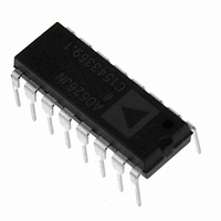
AD526JNZ Analog Devices Inc, AD526JNZ Datasheet - Page 9

AD526JNZ
Manufacturer Part Number
AD526JNZ
Description
IC AMP PGA 10MA 16DIP
Manufacturer
Analog Devices Inc
Type
Programmable Gain Amplifierr
Datasheet
1.AD526JNZ.pdf
(14 pages)
Specifications of AD526JNZ
Amplifier Type
Programmable Gain
Number Of Circuits
1
Slew Rate
24 V/µs
-3db Bandwidth
4MHz
Current - Input Bias
50pA
Voltage - Input Offset
400µV
Current - Supply
10mA
Current - Output / Channel
10mA
Voltage - Supply, Single/dual (±)
±4.5 V ~ 16.5 V
Operating Temperature
0°C ~ 70°C
Mounting Type
Through Hole
Package / Case
16-DIP (0.300", 7.62mm)
No. Of Amplifiers
1
Bandwidth
350kHz
No. Of Channels
1
Supply Voltage Range
± 4.5V To ± 16V
Amplifier Case Style
DIP
No. Of Pins
16
Operating Temperature Range
0°C To +70°C
Number Of Channels
1
Number Of Elements
1
Power Supply Requirement
Dual
Input Offset Voltage
1.5@±15VmV
Single Supply Voltage (typ)
Not RequiredV
Dual Supply Voltage (typ)
±5/±9/±12/±15V
Rail/rail I/o Type
No
Single Supply Voltage (min)
Not RequiredV
Single Supply Voltage (max)
Not RequiredV
Dual Supply Voltage (min)
±4.5V
Dual Supply Voltage (max)
±16.5V
Operating Temp Range
0C to 70C
Operating Temperature Classification
Commercial
Mounting
Through Hole
Pin Count
16
Package Type
PDIP
Lead Free Status / RoHS Status
Lead free / RoHS Compliant
Output Type
-
Gain Bandwidth Product
-
Lead Free Status / Rohs Status
Compliant
Available stocks
Company
Part Number
Manufacturer
Quantity
Price
REV. D
The specifications on page 3, in combination with Figure 35,
give the timing requirements for loading new gain codes.
TIMING AND CONTROL
A2 A1 A0 B
X
0
0
0
0
1
X
X
0
0
0
0
1
NOTE: X = Don’t Care.
Gain Code
X
0
0
1
1
X
X
X
0
0
1
1
X
GAIN CODE
CLK OR CS
INPUTS
T
T
T
X
0
1
0
1
X
X
X
0
1
0
1
X
C
S
H
= DATA SETUP TIME
= MINIMUM CLOCK CYCLE
= DATA HOLD TIME
X
1
1
1
1
1
0
0
1
1
1
1
1
Table I. Logic Input Truth Table
CLK (CS = 0)
Figure 35. AD526 Timing
Control
T
1
0
0
0
0
0
0
1
1
1
1
1
1
C
T
VALID DATA
S
NOTE: THRESHOLD LEVEL FOR
GAIN CODE, CS, AND CLK IS 1.4V.
Condition
Previous State
T
Gain
H
16
16
1
2
4
8
1
1
1
2
4
8
Condition
Latched
Transparent
Transparent
Transparent
Transparent
Transparent
Transparent
Latched
Latched
Latched
Latched
Latched
Latched
–9–
DIGITAL FEEDTHROUGH
With either CS or CLK or both held high, the AD526 gain state
will remain constant regardless of the transitions at the A0, A1,
A2 or B inputs. However, high speed logic transitions will un-
avoidably feed through to the analog circuitry within the AD526
causing spikes to occur at the signal output.
This feedthrough effect can be completely eliminated by operat-
ing the AD526 in the transparent mode and latching the gain
code in an external bank of latches (Figure 36).
To operate the AD526 using serial inputs, the configuration
shown in Figure 36 can be used with the 74LS174 replaced by a
serial-in/parallel-out latch, such as the 54LS594.
Figure 36. Using an External Latch to Minimize Digital
Feedthrough
SIGNAL
TIMING
V
IN
A1
16
A1
1
AD526
16
LOGIC AND LATCHES
A0
15
A0
2
GAIN NETWORK
8
14
CS CLK
74LS174
3
4
13
4
2
A2
A2
12
5
1
11
B
B
6
+
–
–V
+V
10
7
S
S
+5V
9
8
0.1 F
0.1 F
OUT
FORCE
OUT
SENSE
AD526
1 F
V
OUT


