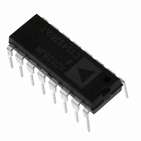
AD526JNZ Analog Devices Inc, AD526JNZ Datasheet - Page 8

AD526JNZ
Manufacturer Part Number
AD526JNZ
Description
IC AMP PGA 10MA 16DIP
Manufacturer
Analog Devices Inc
Type
Programmable Gain Amplifierr
Datasheet
1.AD526JNZ.pdf
(14 pages)
Specifications of AD526JNZ
Amplifier Type
Programmable Gain
Number Of Circuits
1
Slew Rate
24 V/µs
-3db Bandwidth
4MHz
Current - Input Bias
50pA
Voltage - Input Offset
400µV
Current - Supply
10mA
Current - Output / Channel
10mA
Voltage - Supply, Single/dual (±)
±4.5 V ~ 16.5 V
Operating Temperature
0°C ~ 70°C
Mounting Type
Through Hole
Package / Case
16-DIP (0.300", 7.62mm)
No. Of Amplifiers
1
Bandwidth
350kHz
No. Of Channels
1
Supply Voltage Range
± 4.5V To ± 16V
Amplifier Case Style
DIP
No. Of Pins
16
Operating Temperature Range
0°C To +70°C
Number Of Channels
1
Number Of Elements
1
Power Supply Requirement
Dual
Input Offset Voltage
1.5@±15VmV
Single Supply Voltage (typ)
Not RequiredV
Dual Supply Voltage (typ)
±5/±9/±12/±15V
Rail/rail I/o Type
No
Single Supply Voltage (min)
Not RequiredV
Single Supply Voltage (max)
Not RequiredV
Dual Supply Voltage (min)
±4.5V
Dual Supply Voltage (max)
±16.5V
Operating Temp Range
0C to 70C
Operating Temperature Classification
Commercial
Mounting
Through Hole
Pin Count
16
Package Type
PDIP
Lead Free Status / RoHS Status
Lead free / RoHS Compliant
Output Type
-
Gain Bandwidth Product
-
Lead Free Status / Rohs Status
Compliant
Available stocks
Company
Part Number
Manufacturer
Quantity
Price
AD526
THEORY OF OPERATION
The AD526 is a complete software programmable gain amplifier
(SPGA) implemented monolithically with a drift-trimmed
BiFET amplifier, a laser wafer trimmed resistor network, JFET
analog switches and TTL compatible gain code latches.
A particular gain is selected by applying the appropriate gain
code (see Table I) to the control logic. The control logic turns
on the JFET switch that connects the correct tap on the gain
network to the inverting input of the amplifier; all unselected
JFET gain switches are off (open). The “on” resistance of the
gain switches causes negligible gain error since only the
amplifier’s input bias current, which is less than 150 pA, actu-
ally flows through these switches.
The AD526 is capable of storing the gain code, (latched mode),
B, A0, A1, A2, under the direction of control inputs CLK and
CS. Alternatively, the AD526 can respond directly to gain code
changes if the control inputs are tied low (transparent mode).
For gains of 8 and 16, a fraction of the frequency compensation
capacitance (C1 in Figure 32) is automatically switched out of
the circuit. This increases the amplifier’s bandwidth and im-
proves its signal settling time and slew rate.
CLK
Figure 32. Simplified Schematic of the AD526
CS
A0
A1
A2
B
V
IN
A
C
H
L
T
E
S
DIGITAL
GND
O
O
O
G
C
N
T
R
L
L
C
I
ANALOG
N1
GND2
G = 8
G = 16
14k
1k
1k
AMPLIFIER
N2
3.4k
1.7k
1.7k
G = 2
G = 4
ANALOG
GND1
C1
C2
RESISTOR
NETWORK
+V
–V
S
S
OUT
FORCE
OUT
SENSE
–8–
TRANSPARENT MODE OF OPERATION
directly to level changes at the gain code inputs (A0, A1, A2) if
B is tied high and both CS and CLK are allowed to float low.
After the gain codes are changed, the AD526’s output voltage
typically requires 5.5 s to settle to within 0.01% of the final
value. Figures 26 to 29 show the performance of the AD526 for
positive gain code changes.
LATCHED MODE OF OPERATION
The latched mode of operation is shown in Figure 34. When
either CS or CLK go to a Logic “1,” the gain code (A0, A1, A2,
B) signals are latched into the registers and held until both CS
and CLK return to “0.” Unused CS or CLK inputs should be tied
to ground . The CS and CLK inputs are functionally and electri-
cally equivalent.
In the transparent mode of operation, the AD526 will respond
TIMING SIGNAL
V
A2
A1
A0
IN
V
A2
A1
A0
16
A1
IN
1
AD526
16
LOGIC AND LATCHES
A0
15
16
A1
Figure 33. Transparent Mode
2
1
AD526
GAIN NETWORK
Figure 34. Latched Mode
8
16
LOGIC AND LATCHES
A0
14
CS CLK
15
3
2
GAIN NETWORK
4
8
13
14
CS CLK
4
3
2
4
A2
12
13
5
4
1
2
+5V
11
B
12
A2
6
5
1
+
–
–V
+V
+5V
10
11
7
B
6
S
S
+
–
–V
+V
10
9
8
7
0.1 F
0.1 F
S
S
OUT
FORCE
OUT
SENSE
9
8
0.1 F
0.1 F
OUT
FORCE
OUT
SENSE
V
OUT
REV. D
V
OUT


