EM250-BBRD-R Ember, EM250-BBRD-R Datasheet - Page 22
EM250-BBRD-R
Manufacturer Part Number
EM250-BBRD-R
Description
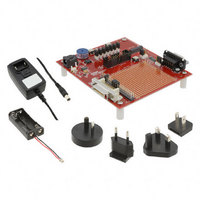
EM250 BREAKOUT BOARD
Manufacturer
Ember
Type
Transceiver, 802.15.4r
Datasheet
1.EM250-RCM-R.pdf
(126 pages)
Specifications of EM250-BBRD-R
Frequency
2.4GHz
For Use With/related Products
EM250
Lead Free Status / RoHS Status
Lead free / RoHS Compliant
Other names
636-1024


EM250
4.7
4.8
120-0082-000S
Encryption Accelerator
nRESET Signal
4.6.2
The Ember stack reserves a section of Flash memory to provide Simulated EEPROM storage area for stack and
customer tokens. Therefore, the EM250 utilizes 8kB of upper Flash storage. This section of Flash is only acces-
sible when mapped to the Flash window in the data-side address space. Because the Flash cells are qualified
for up to 1,000 write cycles, the Simulated EEPROM implements an effective wear-leveling algorithm which ef-
fectively extends the number of write cycles for individual tokens.
4.6.3
The EM250 also includes a separate 1024-byte FIA that can be used for storage of data during manufacturing,
including serial numbers and calibration values. This area is mapped to the data side of the address space,
starting at address 0x5000. While this area can be read as individual bytes, it can only be written to one word
at a time, and may only be erased as a whole. Programming of this special Flash page can only be enabled us-
ing the SIF interface to prevent accidental corruption or erasure. The EmberZNet stack reserves a small por-
tion of this space for its own use, but the rest is available to the application.
4.6.4
The EM250 integrates 5kB of SRAM. Like the Flash memory, this RAM is also mapped to both the program and
data-side address spaces. On the program side, the RAM is mapped to the top 2.5k words of the program ad-
dress space. The program-side mapping of the RAM is used for code when writing to or erasing the Flash mem-
ory. On the data side, the RAM is also mapped to the top of the address space, occupying the last 5kB, as
shown in Figure 3 and Figure 4.
Additionally, the EM250 supports a protection mechanism to prevent application code from overwriting system
data stored in the RAM. To enable this, the RAM is segmented into 32-byte sections, each with a configurable
bit that allows or denies write access when the EM250 is running in Application Mode. Read access is always al-
lowed to the entire RAM, and full access is always allowed when the EM250 is running in System Mode. The
EmberZNet stack intelligently manages this protection mechanism to assist in tracking down many common
application errors.
4.6.5
Table 42 provides a short description of all application-accessible registers within the EM250. Complete de-
scriptions are provided at the end of each applicable Functional Description section. The registers are mapped
to the data-side address space starting at address 0x4000. These registers allow for the control and configura-
tion of the various peripherals and modules. The registers may only be accessed as whole word quantities; at-
tempts to access them as bytes may result in undefined behavior. There are additional registers used by the
EmberZNet stack when the EM250 is running in System Mode, allowing for control of the MAC, baseband, and
other internal modules. These system registers are protected from being modified when the EM250 is running
in Application Mode.
The EM250 contains a hardware AES encryption engine that is attached to the CPU using a memory-mapped in-
terface. NIST-based CCM, CCM*, CBC-MAC, and CTR modes are implemented in hardware. These modes are de-
scribed in the IEEE 802.15.4-2003 specification, with the exception of CCM*, which is described in the ZigBee
Security Services Specification 1.0. The EmberZNet stack implements a security API for applications that re-
quire security at the application level.
When the asynchronous external reset signal, nRESET (Pin 13), is driven low for a time greater than 200ns, the
EM250 resets to its default state. An integrated glitch filter prevents noise from causing an inadvertent reset
to occur. If the EM250 is to be placed in a noisy environment, an external LC Filter or supervisory reset circuit
is recommended to guarantee the integrity of the reset signal.
Simulated EEPROM
Flash Information Area (FIA)
RAM
Registers
Page 22
Related parts for EM250-BBRD-R
Image
Part Number
Description
Manufacturer
Datasheet
Request
R

Part Number:
Description:
IC ZIGBEE SYSTEM-ON-CHIP 48-QFN
Manufacturer:
Ember
Datasheet:

Part Number:
Description:
KIT JUMP START FOR EM250
Manufacturer:
Ember
Datasheet:

Part Number:
Description:
KIT EVAL EM250 RF TEST
Manufacturer:
Ember
Datasheet:

Part Number:
Description:
EM250 RCM BOARD
Manufacturer:
Ember
Datasheet:

Part Number:
Description:
KIT DEV FOR EM250
Manufacturer:
Ember
Datasheet:

Part Number:
Description:
KIT DEV EMBER ZIGBEE W/PCWH
Manufacturer:
Custom Computer Services Inc (CCS)

Part Number:
Description:
PROGRAMMER USB FLASH EM250/260
Manufacturer:
Ember
Datasheet:

Part Number:
Description:
IC ZIGBEE SYSTEM-ON-CHIP 40-QFN
Manufacturer:
Ember
Datasheet:
Part Number:
Description:
IC RF TXRX ZIGBEE 128KB 48QFN
Manufacturer:
Ember
Datasheet:
Part Number:
Description:
IC RF TXRX ZIGBEE 192KB 48QFN
Manufacturer:
Ember
Datasheet:

Part Number:
Description:
INSIGHT ADAPTER FOR EM2XX
Manufacturer:
Ember
Datasheet:

Part Number:
Description:
IAR EWARM LICENCE FOR EM35X
Manufacturer:
Ember
Datasheet:

Part Number:
Description:
INSIGHT ADAPTER 3 FOR EM35X
Manufacturer:
Ember
Datasheet:

Part Number:
Description:
EM35X BREAKOUT BOARD
Manufacturer:
Ember
Datasheet:

Part Number:
Description:
EM260 RCM BOARD
Manufacturer:
Ember
Datasheet: