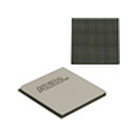
EP2SGX90EF1152I4 Altera, EP2SGX90EF1152I4 Datasheet - Page 142

EP2SGX90EF1152I4
Manufacturer Part Number
EP2SGX90EF1152I4
Description
Stratix II GX
Manufacturer
Altera
Datasheet
1.EP2SGX90EF1152I4.pdf
(316 pages)
Specifications of EP2SGX90EF1152I4
Family Name
Stratix II GX
Number Of Logic Blocks/elements
90960
# I/os (max)
558
Frequency (max)
732.1MHz
Process Technology
SRAM
Operating Supply Voltage (typ)
1.2V
Logic Cells
90960
Ram Bits
4520448
Operating Supply Voltage (min)
1.15V
Operating Supply Voltage (max)
1.25V
Operating Temp Range
-40C to 100C
Operating Temperature Classification
Industrial
Mounting
Surface Mount
Pin Count
1152
Package Type
FC-FBGA
Lead Free Status / Rohs Status
Not Compliant
Available stocks
Company
Part Number
Manufacturer
Quantity
Price
Company:
Part Number:
EP2SGX90EF1152I4
Manufacturer:
ALTERA
Quantity:
745
Company:
Part Number:
EP2SGX90EF1152I4N
Manufacturer:
ALTERA
Quantity:
535
Part Number:
EP2SGX90EF1152I4N
Manufacturer:
ALTERA/阿尔特拉
Quantity:
20 000
- Current page: 142 of 316
- Download datasheet (2Mb)
I/O Structure
2–134
Stratix II GX Device Handbook, Volume 1
Notes to
(1)
(2)
(3)
(4)
V
Table 2–35. Stratix II GX MultiVolt I/O Support
CCIO
1.2
1.5
1.8
2.5
3.3
To drive inputs higher than V
the Allow LVTTL and LVCMOS input levels to overdrive input buffer option in the Quartus II
software.
The pin current may be slightly higher than the default value. You must verify that the driving
device’s V
V
Although V
receiving device powered at a different level can still interface with the Stratix II GX device if it
has inputs that tolerate the V
Stratix II GX devices support 1.2-V HSTL. They do not support 1.2-V LVTTL and 1.2-V LVCMOS.
(V)
I L
maximum and V
Table
1.2
(4)
(4)
(4)
(4)
(4)
Table 2–35
The TDO and nCEO pins are powered by V
TDO is in I/O bank 4 and nCEO is in I/O bank 7. Ideally, the V
for the I/O buffers of any two connected pins are at the same voltage
level. This may not always be possible depending on the V
TDO and nCEO pins on master devices and the configuration voltage level
chosen by V
position in the chain. Master indicates that it is driving out TDO or nCEO
to a slave device. For multi-device passive configuration schemes, the
nCEO pin of the master device drives the nCE pin of the slave device. The
VCCSEL pin on the slave device selects which input buffer is used for nCE.
When V
V
powered by V
in a master device match the V
the slave device it is connected to, but that may not be possible depending
on the application.
O L
2–35:
CCIO
CCIO
maximum and V
v
1.5
specifies the voltage necessary for the Stratix II GX device to drive out, a
. When V
v
v
—
—
(2)
CCSEL
Input Signal (V)
I H
summarizes Stratix II GX MultiVolt I/O support.
minimum voltage specifications.
CCSEL
v
1.8
v
v
is logic high, it selects the 1.8-V/1.5-V buffer powered by
—
—
CCPD
CCSEL
(2)
CCIO
CCIO
O H
on slave devices. Master and slave devices can be in any
. The ideal case is to have the V
value.
minimum voltages do not violate the applicable Stratix II GX
but less than 4.0 V, disable the PCI clamping diode and select
v
v
v
is logic low, it selects the 3.3-V/2.5-V input buffer
2.5
v
v
(2)
(2)
(2)
v
v
v
3.3
v
v
(2)
(2)
(2)
CCSEL
Note (1)
v
v
v
v
v
settings for the nCE input buffer of
1.2
(4)
(3)
(3)
(3)
(3)
CCIO
v
v
v
1.5
—
v
(3)
(3)
(3)
of the bank that they reside.
Output Signal (V)
v
v
CCIO
1.8
v
—
—
(3)
(3)
of the nCEO bank
Altera Corporation
v
2.5
—
—
—
v
CCIO
(3)
October 2007
CC
level of
supplies
3.3 5.0
v
—
—
—
—
—
—
—
—
v
Related parts for EP2SGX90EF1152I4
Image
Part Number
Description
Manufacturer
Datasheet
Request
R

Part Number:
Description:
CYCLONE II STARTER KIT EP2C20N
Manufacturer:
Altera
Datasheet:

Part Number:
Description:
CPLD, EP610 Family, ECMOS Process, 300 Gates, 16 Macro Cells, 16 Reg., 16 User I/Os, 5V Supply, 35 Speed Grade, 24DIP
Manufacturer:
Altera Corporation
Datasheet:

Part Number:
Description:
CPLD, EP610 Family, ECMOS Process, 300 Gates, 16 Macro Cells, 16 Reg., 16 User I/Os, 5V Supply, 15 Speed Grade, 24DIP
Manufacturer:
Altera Corporation
Datasheet:

Part Number:
Description:
Manufacturer:
Altera Corporation
Datasheet:

Part Number:
Description:
CPLD, EP610 Family, ECMOS Process, 300 Gates, 16 Macro Cells, 16 Reg., 16 User I/Os, 5V Supply, 30 Speed Grade, 24DIP
Manufacturer:
Altera Corporation
Datasheet:

Part Number:
Description:
High-performance, low-power erasable programmable logic devices with 8 macrocells, 10ns
Manufacturer:
Altera Corporation
Datasheet:

Part Number:
Description:
High-performance, low-power erasable programmable logic devices with 8 macrocells, 7ns
Manufacturer:
Altera Corporation
Datasheet:

Part Number:
Description:
Classic EPLD
Manufacturer:
Altera Corporation
Datasheet:

Part Number:
Description:
High-performance, low-power erasable programmable logic devices with 8 macrocells, 10ns
Manufacturer:
Altera Corporation
Datasheet:

Part Number:
Description:
Manufacturer:
Altera Corporation
Datasheet:

Part Number:
Description:
Manufacturer:
Altera Corporation
Datasheet:

Part Number:
Description:
Manufacturer:
Altera Corporation
Datasheet:

Part Number:
Description:
CPLD, EP610 Family, ECMOS Process, 300 Gates, 16 Macro Cells, 16 Reg., 16 User I/Os, 5V Supply, 25 Speed Grade, 24DIP
Manufacturer:
Altera Corporation
Datasheet:


