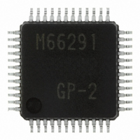
M66291GP#201 Renesas Electronics America, M66291GP#201 Datasheet - Page 64

M66291GP#201
Manufacturer Part Number
M66291GP#201
Description
IC USB CONTROLLER GEN-PUR 48LQFP
Manufacturer
Renesas Electronics America
Datasheet
1.M66291GP201.pdf
(126 pages)
Specifications of M66291GP#201
Package / Case
48-LQFP
Mounting Type
Surface Mount
Current - Supply
30mA
Voltage - Supply
3 V ~ 3.6 V
Operating Temperature
-20°C ~ 85°C
Interface
Serial
Controller Type
USB 2.0 Controller
Lead Free Status / RoHS Status
Not Compliant
Available stocks
Company
Part Number
Manufacturer
Quantity
Price
M 6 6 2 9 1 G P / H P
R e v 1 . 0 1
(1) BUST (Burst Mode) Bit (b15)
(2) DFORM (Transfer Method) Bit (b14~b13)
(3) RWND (Buffer Rewind) Bit (b12)
(4) ACKA (DACK Polarity) Bit (b11)
(5) REQA (DREQ Polarity) Bit (b10)
When set to cycle steal transfer, the assertion and negation of the DREQ signal are repeated every time the
signal is subjected to DMA transfer (8-bit or 16-bit) when the CPU side buffer can be accessed. The negation is
executed when the Dn_FIFO Data Register is accessed.
When set to burst transfer, it keeps on asserting the DREQ signal until the reading/writing of the CPU side
buffer completes when the CPU side buffer can be accessed.
It is possible to forcibly complete the writing and then enabling transmit of short packet by asserting the TC
signal at the time of writing.
These bits select the DMA transfer method.
When the endpoint set to the OUT buffer (EPi_DIR bit = “0”) is assigned to the DMA_EP, writing operation to
the Dn_FIFO Data Register is ignored.
Similarly, when the endpoint set to the IN buffer (EPi_DIR bit = “1”) is assigned to the DMA_EP, reading
operation to the Dn_FIFO Data Register is ignored (undefined value is read).
This bit rewinds (clears) the buffer pointer.
This bit sets the DACK signal polarity.
This bit sets the DREQ signal polarity.
2 0 0 4 . 1 1 . 0 1
When set to “00”
When set to “01”
When set to “10”
When set to OUT buffer (EPi_DIR bit = “0”)
When set to IN buffer (EPi_DIR bit = “1”)
At the time of reading, the data of the Dn_FIFO Data Register is available while the DACK signal is at
“L” and the read signal at “L”.
At the time of writing, the data is written to the Dn_FIFO Data Register when the DACK signal is at
“L” and by the rising edge of write signal.
Only the DACK signal is used and the Read/Write signal is not used (the Read/Write signal is ignored).
At the time of reading, the data of the Dn_FIFO Data Register is available while the DACK signal is at
“L”.
At the time of writing, the data is written to the Dn_FIFO Data Register by the rising edge of DACK
signal.
In place of the DACK signal (the DACK signal is ignored here), the address signal can be used to
read/write the data of the Dn_FIFO Data Register.
At the time of reading, the data of the Dn_FIFO Data Register is available when the read signal is at
“L”.
At the time of writing, the data is written to the Dn_FIFO Data Register by the rising edge of write.
When the IVAL bit of the Dn_FIFO Control Register is set to “1”, the buffer reading pointer can be
cleared by writing “1” to this bit. This enables reading of the receive data from the beginning.
When the IVAL bit of the Dn_FIFO Control Register is set to “0”, the buffer writing pointer can be
cleared by writing “1” to this bit. This enables resetting of the transmit data from the beginning.
p a g e 6 4 o f 1 2 2


