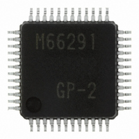
M66291GP#201 Renesas Electronics America, M66291GP#201 Datasheet - Page 68

M66291GP#201
Manufacturer Part Number
M66291GP#201
Description
IC USB CONTROLLER GEN-PUR 48LQFP
Manufacturer
Renesas Electronics America
Datasheet
1.M66291GP201.pdf
(126 pages)
Specifications of M66291GP#201
Package / Case
48-LQFP
Mounting Type
Surface Mount
Current - Supply
30mA
Voltage - Supply
3 V ~ 3.6 V
Operating Temperature
-20°C ~ 85°C
Interface
Serial
Controller Type
USB 2.0 Controller
Lead Free Status / RoHS Status
Not Compliant
Available stocks
Company
Part Number
Manufacturer
Quantity
Price
M 6 6 2 9 1 G P / H P
R e v 1 . 0 1
(3) IVAL (IN Buffer Set/OUT Buffer Status) Bit (b13)
(4) BCLR (Buffer Clear) Bit (b12)
(5) Dreq (D_FIFO Ready) Bit (b11)
(6) DMA_DTLN (D_FIFO Receive Data Length Register) Bits (b10~b0)
This bit indicates valid value when the Dreq bit of this register is equal to “0”.
The operation of this bit is the same as that of the IVAL bit of the CPU_FIFO Control Register.
Take care the setting of the EPB_RDY bit to “1” using this bit (buffer ready interrupt occurs) changes
according to the INTM bit (Refer to “EPB_RDY/INTM bit”).
This bit indicates valid value when the Dreq bit of this register is set to “0”.
The operation of this bit is the same as that of the BCLR bit of the CPU_FIFO Control Register.
When this bit is equal to “1”, this bit indicates the states as follows:
Make sure that this bit is equal to “0” before making access to the aforesaid registers/bits.
These bits are valid against the endpoint set to the OUT buffer (EPi_DIR bit = “0”) and indicates the receive
data number (byte count) in the CPU side buffer.
These bits indicate the valid value when the Dreq bit of this register is equal to “0”.
2 0 0 4 . 1 1 . 0 1
Note:
•
•
•
Refer to “3.2 FIFO Buffer” for CPU/SIE side.
Dn_FIFO Data Register can not be accessed.
The IVAL bit value of this register is invalid.
The DMA_DTLN bit values of this register are invalid.
p a g e 6 8 o f 1 2 2


