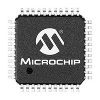
PIC24FV32KA304-I/PT Microchip Technology, PIC24FV32KA304-I/PT Datasheet - Page 14

PIC24FV32KA304-I/PT
Manufacturer Part Number
PIC24FV32KA304-I/PT
Description
MCU 32KB FLASH 2KB RAM 44-TQFP
Manufacturer
Microchip Technology
Specifications of PIC24FV32KA304-I/PT
Processor Series
PIC24FV
Core
PIC
Data Bus Width
16 bit
Program Memory Type
Flash
Program Memory Size
32 KB
Data Ram Size
2 KB
Maximum Operating Temperature
+ 85 C
Mounting Style
SMD/SMT
Package / Case
TQFP-44
Development Tools By Supplier
MPLAB IDE Software
Minimum Operating Temperature
- 40 C
Lead Free Status / Rohs Status
Lead free / RoHS Compliant
Available stocks
Company
Part Number
Manufacturer
Quantity
Price
Company:
Part Number:
PIC24FV32KA304-I/PT
Manufacturer:
VISHAY
Quantity:
12 000
Company:
Part Number:
PIC24FV32KA304-I/PT
Manufacturer:
Microchip Technology
Quantity:
10 000
- Current page: 14 of 320
- Download datasheet (3Mb)
PIC24FV32KA304 FAMILY
The internal oscillator block also provides a stable
reference source for the Fail-Safe Clock Monitor
(FSCM). This option constantly monitors the main clock
source against a reference signal provided by the
internal oscillator and enables the controller to switch to
the internal oscillator, allowing for continued low-speed
operation or a safe application shutdown.
1.1.4
Regardless of the memory size, all the devices share
the same rich set of peripherals, allowing for a smooth
migration path as applications grow and evolve.
The consistent pinout scheme used throughout the
entire family also helps in migrating to the next larger
device. This is true when moving between devices with
the same pin count, or even jumping from 20-pin or
28-pin devices to 44-pin/48-pin devices.
The PIC24F family is pin compatible with devices in the
dsPIC33 family, and shares some compatibility with the
pinout schema for PIC18 and dsPIC30. This extends
the ability of applications to grow from the relatively
simple, to the powerful and complex.
1.2
• Communications: The PIC24FV32KA304 family
• Real-Time Clock/Calendar: This module
• 12-Bit A/D Converter: This module incorporates
• Charge Time Measurement Unit (CTMU)
DS39995B-page 14
incorporates a range of serial communication
peripherals to handle a range of application
requirements. There is an I
supports both the Master and Slave modes of
operation. It also comprises UARTs with built-in
IrDA
implements a full-featured clock and calendar with
alarm functions in hardware, freeing up timer
resources and program memory space for use of
the core application.
programmable acquisition time, allowing for a
channel to be selected and a conversion to be
initiated without waiting for a sampling period, and
faster sampling speed. The 16-deep result buffer
can be used either in Sleep to reduce power, or in
Active mode to improve throughput.
Interface: The PIC24FV32KA304 family includes
the new CTMU interface module, which can be
used for capacitive touch sensing, proximity
sensing, and also for precision time measurement
and pulse generation.
®
encoders/decoders and an SPI module.
Other Special Features
EASY MIGRATION
2
C™ module that
1.3
Devices in the PIC24FV32KA304 family are available
in 20-pin, 28-pin, 44-pin and 48-pin packages. The
general block diagram for all devices is shown in
Figure
The devices are different from each other in four ways:
1.
2.
3.
4.
All other features for devices in this family are identical;
these are summarized in
A
PIC24FV32KA304 family devices, sorted by function,
is provided in
Note:
list
Flash
PIC24FV16KA
PIC24FV32KA devices).
Available I/O pins and ports (18 pins on two
ports for 20-pin devices, 22 pins on two ports for
28-pin devices and 38 pins on three ports for
44/48-pin devices).
Alternate SCL and SDA pins are available only
in 28-pin, 44-pin and 48-pin devices and not in
20-pin devices.
Members of the PIC24FV32KA301 family are
available as both standard and high-voltage
devices. High-voltage devices designated with
an “FV” in the part number (such as
PIC24FV32KA304), accommodate an operating
V
on-board voltage regulator that powers the core.
Peripherals operate at V
designated by “F” (such as PIC24F32KA304),
function over a lower V
These parts do not have an internal regulator,
and both the core and peripherals operate
directly from V
DD
1-1.
Details on Individual Family
Members
of
range of 2.0V to 5.5V, and have an
Table 1-1
individual peripheral features and not how
they are multiplexed on the same pin. This
information is provided in the pinout
diagrams on pages 5, 5, 6, 7,
the data sheet. Multiplexed features are
sorted by the priority given to a feature,
with the highest priority peripheral being
listed first.
program
the
Table
DD
pin
.
.
devices,
provides the pin location of
memory
2011 Microchip Technology Inc.
features
Table
DD
DD
range of 1.8V to 3.6V.
1-1.
. Standard devices,
32
(16
available
Kbytes
Kbytes
8
and
on
for
9
for
the
of
Related parts for PIC24FV32KA304-I/PT
Image
Part Number
Description
Manufacturer
Datasheet
Request
R

Part Number:
Description:
Manufacturer:
Microchip Technology Inc.
Datasheet:

Part Number:
Description:
Manufacturer:
Microchip Technology Inc.
Datasheet:

Part Number:
Description:
Manufacturer:
Microchip Technology Inc.
Datasheet:

Part Number:
Description:
Manufacturer:
Microchip Technology Inc.
Datasheet:

Part Number:
Description:
Manufacturer:
Microchip Technology Inc.
Datasheet:

Part Number:
Description:
Manufacturer:
Microchip Technology Inc.
Datasheet:

Part Number:
Description:
Manufacturer:
Microchip Technology Inc.
Datasheet:

Part Number:
Description:
Manufacturer:
Microchip Technology Inc.
Datasheet:


