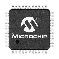
PIC24FV32KA304-I/PT Microchip Technology, PIC24FV32KA304-I/PT Datasheet - Page 142

PIC24FV32KA304-I/PT
Manufacturer Part Number
PIC24FV32KA304-I/PT
Description
MCU 32KB FLASH 2KB RAM 44-TQFP
Manufacturer
Microchip Technology
Specifications of PIC24FV32KA304-I/PT
Processor Series
PIC24FV
Core
PIC
Data Bus Width
16 bit
Program Memory Type
Flash
Program Memory Size
32 KB
Data Ram Size
2 KB
Maximum Operating Temperature
+ 85 C
Mounting Style
SMD/SMT
Package / Case
TQFP-44
Development Tools By Supplier
MPLAB IDE Software
Minimum Operating Temperature
- 40 C
Lead Free Status / Rohs Status
Lead free / RoHS Compliant
Available stocks
Company
Part Number
Manufacturer
Quantity
Price
Company:
Part Number:
PIC24FV32KA304-I/PT
Manufacturer:
VISHAY
Quantity:
12 000
Company:
Part Number:
PIC24FV32KA304-I/PT
Manufacturer:
Microchip Technology
Quantity:
10 000
- Current page: 142 of 320
- Download datasheet (3Mb)
PIC24FV32KA304 FAMILY
11.2.2
One instruction cycle is required between a port
direction change or port write operation and a read
operation of the same port. Typically, this instruction
would be a NOP.
11.3
The input change notification function of the I/O ports
allows the PIC24FV32KA304 family of devices to
generate interrupt requests to the processor in
response to a Change-of-State (COS) on selected
input pins. This feature is capable of detecting input
change of states, even in Sleep mode, when the clocks
are disabled. Depending on the device pin count, there
are up to 23 external signals (CN0 through CN22) that
may be selected (enabled) for generating an interrupt
request on a Change-of-State.
There are six control registers associated with the CN
module. The CNEN1 and CNEN2 registers contain the
interrupt enable control bits for each of the CN input
pins. Setting any of these bits enables a CN interrupt
for the corresponding pins.
Each CN pin also has a weak pull-up/pull-down
connected to it. The pull-ups act as a current source
that is connected to the pin. The pull-downs act as a
current sink to eliminate the need for external resistors
when push button or keypad devices are connected.
EXAMPLE 11-1:
DS39995B-page 142
MOV
MOV
NOP;
BTSS
Equivalent ‘C’ Code
TRISB = 0xFF00;
NOP();
if(PORTBbits.RB13 == 1)
{
}
Input Change Notification
0xFF00, W0;
W0, TRISB;
PORTB, #13;
I/O PORT WRITE/READ TIMING
PORT WRITE/READ EXAMPLE
//Configure PORTB<15:8> as inputs and PORTB<7:0> as outputs
//Delay 1 cycle
//Next Instruction
//Configure PORTB<15:8> as inputs and PORTB<7:0> as outputs
//Delay 1 cycle
// execute following code if PORTB pin 13 is set.
On any pin, only the pull-up resistor or the pull-down
resistor should be enabled, but not both of them. If the
push button or the keypad is connected to V
the pull-down, or if they are connected to V
the pull-up resistors. The pull-ups are enabled
separately using the CNPU1 and CNPU2 registers,
which contain the control bits for each of the CN pins.
Setting any of the control bits enables the weak
pull-ups for the corresponding pins. The pull-downs are
enabled separately, using the CNPD1 and CNPD2
registers, which contain the control bits for each of the
CN pins. Setting any of the control bits enables the
weak pull-downs for the corresponding pins.
When the internal pull-up is selected, the pin uses V
as the pull-up source voltage. When the internal
pull-down is selected, the pins are pulled down to V
by an internal resistor. Make sure that there is no
external pull-up source/pull-down sink when the
internal pull-ups/pull-downs are enabled.
Note:
Pull-ups and pull-downs on change notifi-
cation pins should always be disabled
whenever the port pin is configured as a
digital output.
2011 Microchip Technology Inc.
DD
SS
, enable
, enable
DD
SS
Related parts for PIC24FV32KA304-I/PT
Image
Part Number
Description
Manufacturer
Datasheet
Request
R

Part Number:
Description:
Manufacturer:
Microchip Technology Inc.
Datasheet:

Part Number:
Description:
Manufacturer:
Microchip Technology Inc.
Datasheet:

Part Number:
Description:
Manufacturer:
Microchip Technology Inc.
Datasheet:

Part Number:
Description:
Manufacturer:
Microchip Technology Inc.
Datasheet:

Part Number:
Description:
Manufacturer:
Microchip Technology Inc.
Datasheet:

Part Number:
Description:
Manufacturer:
Microchip Technology Inc.
Datasheet:

Part Number:
Description:
Manufacturer:
Microchip Technology Inc.
Datasheet:

Part Number:
Description:
Manufacturer:
Microchip Technology Inc.
Datasheet:


