PIC24FV32KA304-I/PT Microchip Technology, PIC24FV32KA304-I/PT Datasheet - Page 193
PIC24FV32KA304-I/PT
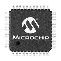
Manufacturer Part Number
PIC24FV32KA304-I/PT
Description
MCU 32KB FLASH 2KB RAM 44-TQFP
Manufacturer
Microchip Technology
Specifications of PIC24FV32KA304-I/PT
Processor Series
PIC24FV
Core
PIC
Data Bus Width
16 bit
Program Memory Type
Flash
Program Memory Size
32 KB
Data Ram Size
2 KB
Maximum Operating Temperature
+ 85 C
Mounting Style
SMD/SMT
Package / Case
TQFP-44
Development Tools By Supplier
MPLAB IDE Software
Minimum Operating Temperature
- 40 C
Lead Free Status / Rohs Status
Lead free / RoHS Compliant
Available stocks
Company
Part Number
Manufacturer
Quantity
Price
Company:

Part Number:
PIC24FV32KA304-I/PT
Manufacturer:
VISHAY
Quantity:
12 000
Company:
Part Number:
PIC24FV32KA304-I/PT
Manufacturer:
Microchip Technology
Quantity:
10 000


REGISTER 19-2:
2011 Microchip Technology Inc.
bit 15
bit 7
Legend:
R = Readable bit
-n = Value at POR
bit 15
bit 14
bit 13
bit 12
bit 11-10
bit 9-8
bit 7-0
Note 1:
PWCEN
R/W-0
U-0
—
2:
The RTCPWC register is only affected by a POR.
When a new value is written to these register bits, the Seconds Value register should also be written to
properly reset the clock prescalers in the RTCC.
PWCEN: Power Control Enable bit
1 = Power control is enabled
0 = Power control is disabled
PWCPOL: Power Control Polarity bit
PWCCPRE: Power Control Control/Stability Prescaler bits
PWCSPRE: Power Control Sample Prescaler bits
RTCCLK<1:0>: RTCC Clock Select bits
Determines the source of the internal RTCC clock, which is used for all RTCC timer operations.
00 = External Secondary Oscillator (SOSC)
01 = Internal LPRC oscillator
10 = External power line source – 50 Hz
11 = External power line source – 60 Hz
RTCOUT<1:0>: RTCC Output Select bits
Determines the source of the RTCC pin output.
00 = RTCC alarm pulse
01 = RTCC seconds clock
10 = RTCC clock
11 = Power control
Unimplemented: Read as ‘0’
1 = Power control output is active-high
0 = Power control output is active-low
1 = PWC stability window clock is divide-by-2 of source RTCC clock
0 = PWC stability window clock is divide-by-1 of source RTCC clock
1 = PWC sample window clock is divide-by-2 of source RTCC clock
0 = PWC sample window clock is divide-by-1 of source RTCC clock
PWCPOL
R/W-0
U-0
—
RTCPWC: RTCC CONFIGURATION REGISTER 2
W = Writable bit
‘1’ = Bit is set
PWCCPRE
R/W-0
U-0
—
PWCSPRE
R/W-0
U-0
—
PIC24FV32KA304 FAMILY
(2)
U = Unimplemented bit, read as ‘0’
‘0’ = Bit is cleared
RTCCLK1
R/W-0
U-0
—
(2)
RTCCLK0
R/W-0
U-0
—
(1)
(2)
x = Bit is unknown
RTCOUT1
R/W-0
U-0
—
DS39995B-page 193
RTCOUT0
R/W-0
U-0
—
bit 0
bit 8
Related parts for PIC24FV32KA304-I/PT
Image
Part Number
Description
Manufacturer
Datasheet
Request
R

Part Number:
Description:
Manufacturer:
Microchip Technology Inc.
Datasheet:
Part Number:
Description:
Manufacturer:
Microchip Technology Inc.
Datasheet:
Part Number:
Description:
Manufacturer:
Microchip Technology Inc.
Datasheet:
Part Number:
Description:
Manufacturer:
Microchip Technology Inc.
Datasheet:
Part Number:
Description:
Manufacturer:
Microchip Technology Inc.
Datasheet:
Part Number:
Description:
Manufacturer:
Microchip Technology Inc.
Datasheet:
Part Number:
Description:
Manufacturer:
Microchip Technology Inc.
Datasheet:
Part Number:
Description:
Manufacturer:
Microchip Technology Inc.
Datasheet: