LMH2190TM-38/NOPB National Semiconductor, LMH2190TM-38/NOPB Datasheet
LMH2190TM-38/NOPB
Specifications of LMH2190TM-38/NOPB
Available stocks


Related parts for LMH2190TM-38/NOPB


LMH2190TM-38/NOPB Summary of contents
Page 1
... The LMH2190 quad clock distributor is offered in a tiny 1.615mm x 1.615mm 16 bump microSMD package. Its small size and low supply current make it ideal for portable appli- cations. Typical Application © 2011 National Semiconductor Corporation LMH2190 Features ■ 1 input clock, 4 output clocks ■ ...
Page 2
... Absolute Maximum Ratings If Military/Aerospace specified devices are required, please contact the National Semiconductor Sales Office/ Distributors for availability and specifications. Supply Voltage BAT SS LVCMOS port IO voltage Current on CLKx pins ESD Tolerance (Note 2) Human Body Model Machine Model Storage Temperature Range Junction Temperature ...
Page 3
Symbol Parameter Jitter Additive RMS period Jitter RMS Phase CLK1 Additive Phase Noise with Noise all Outputs toggling CLK2 Additive Phase Noise with all Outputs toggling CLK3 Additive Phase Noise with all Outputs toggling CLK4 Additive Phase Noise with all ...
Page 4
Symbol Parameter Clock Request Output (SCLK_REQ) tp Propagation Delay, Push-Pull LH and Open Source, Figure (Note 7) tp Propagation Delay, Push-Pull HL and Open Drain, Figure 2, (Note 7) V SCLK_REQ Output Voltage High OH Level V SCLK_REQ Output Voltage ...
Page 5
Symbol Parameter PSRR Power Supply Rejection Ratio E Output Noise Voltage N T Thermal Shutdown SHTDWN ΔV Line Transient (Note 7) OUT Load Transient (Note 7) Overshoot on Startup (Note R DC Output Resistance OUT T Turn on Time (Note ...
Page 6
Timing Waveforms FIGURE 3. Rise / Fall Time and Duty Cycle Waveform for Clock Outputs www.national.com FIGURE 1. Clock Output Timing Waveforms FIGURE 2. Clock Request Timing Waveforms 30083808 FIGURE 4. Setup Time from SCLK_IN to CLK_REQ 6 30083805 30083806 ...
Page 7
... A1 V Battery / BAT Input B1 V LDO / Output OUT B2 V Ground Input Output, I/O = Input / Output 16–Bump micro SMD Marking AA = LMH2190TM-38 30083803 Type Description I Source Clock Input O Source Clock Request O Clock Output 1 I Clock Request Input 1 O Clock Output 2 I Clock Request Input 2 ...
Page 8
... Ordering Information Package Part Number LMH2190TM-38 16-Bump Thin microSMD LMH2190TMX-38 Note: For other addresses please contact your local sales office. Block Diagram www.national.com Package Address Marking 250 Units Tape and Reel 38 AA 3000 Units Tape and Reel LMH2190 8 Transport Media NSC Drawing ...
Page 9
Typical Performance Characteristics 26 MHz 2.2 µ 1.8V (See OUT DD_IO Supply Current vs. Supply Voltage Supply Current vs. Capacitive Load LDO Output Voltage vs. LDO Output Current Unless otherwise specified, T Block Diagram), Registers are ...
Page 10
Additive Phase Noise vs. Frequency Offset CLK1 Response, C CLK1 Response, C www.national.com 30083830 = 22pF L 30083835 = 50 pF Power Supply Rejection Ratio vs. Frequency L 30083837 10 CLK1 Response 30083834 CLK1 Response, ...
Page 11
Application Information The LMH2190 is a quad channel configurable clock distribu- tion device which supplies a digital system clock to peripher- als in mobile handsets or other applications. Examples of peripherals are Bluetooth, Wireless LAN, and/or Digital Video Broadcast-H (DVB-H). ...
Page 12
PHASE NOISE An important specification for oscillators and clock buffers is phase noise. It determines the timing and thus accuracy of various peripheral devices in a cell phone such as Bluetooth, WLAN and DVB-H. Phase noise is expressed in the ...
Page 13
Outputs with Skew only CLOCK REQUEST LOGIC The clock request logic enables an independent control of the clock tree driver outputs (CLK1 to CLK4) as well as an overall source clock request (SCLK_REQ) and LDO enabling. Since the clock ...
Page 14
LDO voltage of 1.8V, but not more than the supply voltage ( the LMH2190. BAT The System Clock Request Output pin can be used to enable or disable an external TCXO to save power ...
Page 15
The LDO contains thermal overheating detection does overheat, the LMH2190 (except the register logic) will shut- down and sets a status bit in the status register. The LDO can be configured to be always ON ...
Page 16
Transferring Data Every frame on the SDA line must be eight bits long, with the most significant bit (MSB) being transferred first. Each byte of data has to be followed by an acknowledge bit. The acknowl- edge related clock pulse ...
Page 17
Timing The timing of the SDA and SCL signals is depicted in Symbol f Clock Frequency SCL 1 Hold Time (repeated) START Condition 2 Clock Low Time 3 Clock High Time 4 Setup Time for a Repeated ...
Page 18
Registers Address = 00H, type = R/W, reset value = 44H, 0100_0100, Bold face settings are the default configuration. Field Output Mode Clock Request Output Type Clock Request Output Polarity Clock Request Output Mode Clock Input Type ...
Page 19
Address = 02H, type = R/W, reset value = 06H, 0000_0110, Bold face settings are the default configuration. Field Bits CLK2 Load [1-0] CLK_REQ2 Input Polarity CLK_REQ2 Force ON Control CLK_REQ2 Force OFF Control CLK_REQ2 Pull down Resistor Reserved Reserved ...
Page 20
Address = 04H, type = R/W, reset value = 06H, 0000_0110, Bold face settings are the default configuration. Field CLK4 Load CLK_REQ4 Input Polarity CLK_REQ4 Force ON Control CLK_REQ4 Force OFF Control CLK_REQ4 Pull down Resistor Reserved Reserved Address = ...
Page 21
LAYOUT RECOMMENDATIONS As with any other device, careful attention must be paid to the board layout. If the board isn't properly designed, the perfor- mance of the device can be less than might be expected. Especially the input clock trace ...
Page 22
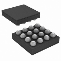
Physical Dimensions X1 = 1.615 ± 0.030 mm 1.615 ± 0.030 mm 0.600 ± 0.075 mm www.national.com inches (millimeters) unless otherwise noted 16-Bump micro SMD NS Package Number TMD16AAA 22 ...
Page 23
Notes 23 www.national.com ...
Page 24
... For more National Semiconductor product information and proven design tools, visit the following Web sites at: www.national.com Products Amplifiers www.national.com/amplifiers Audio www.national.com/audio Clock and Timing www.national.com/timing Data Converters www.national.com/adc Interface www.national.com/interface LVDS www.national.com/lvds Power Management www.national.com/power Switching Regulators www.national.com/switchers LDOs www.national.com/ldo LED Lighting www ...