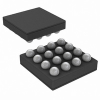
LMH2190TM-38/NOPB National Semiconductor, LMH2190TM-38/NOPB Datasheet - Page 15

LMH2190TM-38/NOPB
Manufacturer Part Number
LMH2190TM-38/NOPB
Description
IC CLOCK QUAD 26MHZ DVR 16-USMD
Manufacturer
National Semiconductor
Type
Fanout Buffer (Distribution)r
Datasheet
1.LMH2190TM-38NOPB.pdf
(24 pages)
Specifications of LMH2190TM-38/NOPB
Number Of Circuits
1
Ratio - Input:output
1:4
Differential - Input:output
No/No
Input
Clock
Output
Clock
Frequency - Max
27MHz
Voltage - Supply
2.5 V ~ 5.5 V
Operating Temperature
-20°C ~ 85°C
Mounting Type
Surface Mount
Package / Case
16-MicroSMD
Frequency-max
27MHz
Lead Free Status / RoHS Status
Lead free / RoHS Compliant
Other names
LMH2190TM-38TR
Available stocks
Company
Part Number
Manufacturer
Quantity
Price
Company:
Part Number:
LMH2190TM-38/NOPB
Manufacturer:
NS
Quantity:
270
The LDO contains thermal overheating detection. If it does
overheat, the LMH2190 (except the register logic) will shut-
down and sets a status bit in the I
The LDO can be configured to be always ON for the case
when it needs to supply power to the TCXO even when the
LMH2190 is not requesting any clocks to be distributed.
It is possible to use an external 1.8V supply connected to
V
ommended to use the internally generated 1.8V. If an external
supply is used, care should be taken during startup as the
default configuration is for the internal LDO to be enabled. In
this case, there could be contention between the two supplies
which could cause excessive current flow.
I
The LMH2190 can be controlled by a I
I
isters inside the LMH2190 to change the default configura-
tion. The I
structure, following the I
to the I
be present on the I
Some of the features are for instance setting the polarity of
the clock request inputs and outputs and setting the drive
strength of the clock outputs. It also allows direct control of
the clock request signals and the LDO via the I
interface is powered by the ENABLE, while the control logic
and registers are powered by the V
I
The data on SDA line must be stable during the HIGH period
of the clock signal (SCL). In other words, the state of the data
line should only change when SCL is LOW
2
2
2
OUT
C CONTROL LOGIC
C address of the LMH2190 is 38h. It can configure the reg-
C Data Validity
and shut off the internal LDO, although it is highly rec-
2
C specification one set of pull-up resistors needs to
2
C communication is based on a READ/WRITE
2
C bus.
2
C transmission protocol. According
2
C status register.
BAT
.
2
FIGURE 11. Linear Regulator Block Diagram
C host device. The
(Figure
2
C. The I
12).
2
C
15
I
START and STOP bits classify the beginning and the end of
the I
transitioning from HIGH to LOW while SCL line is HIGH
ure
from LOW to HIGH while SCL is HIGH. The I
generates START and STOP bits. The I
to be busy after START condition and free after STOP con-
dition. During data transmission, I
repeated START conditions. First START and repeated
START conditions are equivalent, function-wise.
2
C Start and Stop Condition
13). STOP condition is defined as the SDA transitioning
2
C session. START condition is defined as SDA signal
FIGURE 13. I
FIGURE 12. I
2
C Start and Stop Conditions
2
C Signals: Data Validity
30083826
2
C master can generate
2
C bus is considered
2
C master always
www.national.com
30083821
30083822
(Fig-


