LMH2190TM-38/NOPB National Semiconductor, LMH2190TM-38/NOPB Datasheet - Page 16
LMH2190TM-38/NOPB
Manufacturer Part Number
LMH2190TM-38/NOPB
Description
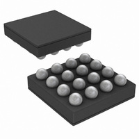
IC CLOCK QUAD 26MHZ DVR 16-USMD
Manufacturer
National Semiconductor
Type
Fanout Buffer (Distribution)r
Datasheet
1.LMH2190TM-38NOPB.pdf
(24 pages)
Specifications of LMH2190TM-38/NOPB
Number Of Circuits
1
Ratio - Input:output
1:4
Differential - Input:output
No/No
Input
Clock
Output
Clock
Frequency - Max
27MHz
Voltage - Supply
2.5 V ~ 5.5 V
Operating Temperature
-20°C ~ 85°C
Mounting Type
Surface Mount
Package / Case
16-MicroSMD
Frequency-max
27MHz
Lead Free Status / RoHS Status
Lead free / RoHS Compliant
Other names
LMH2190TM-38TR
Available stocks
Company
Part Number
Manufacturer
Quantity
Price
Company:

Part Number:
LMH2190TM-38/NOPB
Manufacturer:
NS
Quantity:
270


www.national.com
Transferring Data
Every frame on the SDA line must be eight bits long, with the
most significant bit (MSB) being transferred first. Each byte of
data has to be followed by an acknowledge bit. The acknowl-
edge related clock pulse is generated by the master. The
transmitter releases the SDA line (HIGH) during the acknowl-
edge clock pulse. The receiver must pull down the SDA line
during the 9th clock pulse, signifying an acknowledge. A re-
ceiver which has been addressed must generate an acknowl-
edge after each byte has been received.
After the START condition, the I
dress
an eight bit which is a data direction bit (R/W). For the eighth
bit, a “0” indicates a WRITE and a “1” indicates a READ. The
second byte selects the register to which the data will be writ-
ten. The third byte contains data to write to the selected
register.
(Figure
14). This address is seven bits long followed by
2
C master sends a chip ad-
FIGURE 15. Example I
FIGURE 16. Example I
16
Register changes take effect at the SCL rising edge during
the last ACK from slave. An example of a WRITE cycle is
given in
plished, a WRITE function must precede the READ function,
as shown in the Read Cycle waveform
2
2
C Write Cycle
C Read Cycle
Figure
FIGURE 14. I
15. When a READ function is to be accom-
2
C Chip Address
(Figure
30083823
16).
30083820
30083824
Related parts for LMH2190TM-38/NOPB
Image
Part Number
Description
Manufacturer
Datasheet
Request
R

Part Number:
Description:
Quad Channel 27 MHz Clock Tree Driver with I2C Interface
Manufacturer:
NSC [National Semiconductor]
Datasheet:
Part Number:
Description:
Lmh2190 Quad Channel 27 Mhz Clock Tree Driver With I2c Interface
Manufacturer:
National Semiconductor Corporation
Datasheet:

Part Number:
Description:
National Semiconductor [8-Bit D/A Converter]
Manufacturer:
National Semiconductor
Datasheet:
Part Number:
Description:
National Semiconductor [Media Coprocessor]
Manufacturer:
National Semiconductor
Datasheet:
Part Number:
Description:
Digitally Controlled Tone and Volume Circuit with Stereo Audio Power Amplifier, Microphone Preamp Stage and National 3D Sound
Manufacturer:
National Semiconductor
Datasheet:
Part Number:
Description:
Digitally Controlled Tone and Volume Circuit with Stereo Audio Power Amplifier, Microphone Preamp Stage and National 3D Sound
Manufacturer:
National Semiconductor
Datasheet:
Part Number:
Description:
AC97 Rev 2 Codec with Sample Rate Conversion and National 3D Sound
Manufacturer:
National Semiconductor
Part Number:
Description:
Manufacturer:
National Semiconductor
Datasheet:
Part Number:
Description:
Manufacturer:
National Semiconductor
Datasheet:
Part Number:
Description:
General Purpose, Low Voltage, Low Power, Rail-to-Rail Output Operational Amplifiers
Manufacturer:
National Semiconductor
Datasheet:
Part Number:
Description:
8-bit 20 MSPS flash A/D converter.
Manufacturer:
National Semiconductor
Datasheet:
Part Number:
Description:
Low Noise Quad Operational Amplifier
Manufacturer:
National Semiconductor
Datasheet:
Part Number:
Description:
Quad Differential Line Receivers
Manufacturer:
National Semiconductor
Datasheet:
Part Number:
Description:
Quad High Speed Trapezoidal? Bus Transceiver
Manufacturer:
National Semiconductor
Datasheet: