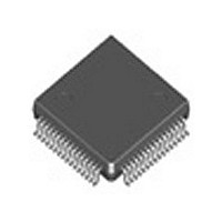
IDT82V3355TF IDT, Integrated Device Technology Inc, IDT82V3355TF Datasheet - Page 14

IDT82V3355TF
Manufacturer Part Number
IDT82V3355TF
Description
Manufacturer
IDT, Integrated Device Technology Inc
Datasheet
1.IDT82V3355TF.pdf
(135 pages)
Specifications of IDT82V3355TF
Function
Wan PLL
Operating Temperature (max)
85C
Operating Temperature (min)
-40C
Package Type
TQFP
Pin Count
64
Mounting
Surface Mount
Lead Free Status / Rohs Status
Not Compliant
Available stocks
Company
Part Number
Manufacturer
Quantity
Price
Company:
Part Number:
IDT82V3355TFG
Manufacturer:
IDT, Integrated Device Technology Inc
Quantity:
10 000
Company:
Part Number:
IDT82V3355TFG8
Manufacturer:
IDT, Integrated Device Technology Inc
Quantity:
10 000
Table 1: Pin Description (Continued)
Pin Description
IDT82V3355
MFRSYNC_2K
FRSYNC_8K
OUT1_POS
OUT1_NEG
IN3_CMOS
INT_REQ
IN2_POS
IN2_NEG
Name
OUT2
CLKE
SCLK
SDO
SDI
CS
Pin No.
25
26
34
17
18
19
20
56
44
43
42
52
47
5
pull-down
pull-down
pull-down
pull-down
pull-up
I/O
I/O
O
O
O
O
O
I
I
I
I
I
PECL/LVDS
PECL/LVDS
CMOS
CMOS
CMOS
CMOS
CMOS
CMOS
CMOS
CMOS
CMOS
Type
Output Frame Synchronization Signal
Microprocessor Interface
IN2_POS / IN2_NEG: Positive / Negative Input Clock 2
A 2 kHz, 4 kHz, N x 8 kHz
25.92 MHz, 38.88 MHz, 51.84 MHz, 77.76 MHz, 155.52 MHz, 156.25 MHz, 311.04 MHz or
622.08 MHz clock is differentially input on this pair of pins. Whether the clock signal is PECL
or LVDS is automatically detected.
Single-ended input for differential input is also supported. Refer to
Ended Input for Differential
IN3_CMOS: Input Clock 3
A 2 kHz, 4 kHz, N x 8 kHz
25.92 MHz, 38.88 MHz, 51.84 MHz, 77.76 MHz or 155.52 MHz clock is input on this pin.
FRSYNC_8K: 8 kHz Frame Sync Output
An 8 kHz signal is output on this pin.
MFRSYNC_2K: 2 kHz Multiframe Sync Output
A 2 kHz signal is output on this pin.
OUT1_POS / OUT1_NEG: Positive / Negative Output Clock 1
A 1 Hz, 400 Hz, 2 kHz, 8 kHz, 64 kHz, N x E1
5 MHz, 10 MHz, 20 MHz, 25 MHz, E3, T3, 6.48 MHz, 19.44 MHz, 25.92 MHz, 38.88 MHz,
51.84 MHz, 77.76 MHz, 125 MHz, 155.52 MHz, 156.25 MHz, 311.04 MHz, 312.5 MHz or
622.08 MHz clock is differentially output on this pair of pins.
OUT2: Output Clock 2
A 1 Hz, 400 Hz, 2 kHz, 8 kHz, 64 kHz, N x E1
5 MHz, 10 MHz, 20 MHz, 25 MHz, E3, T3, 6.48 MHz, 19.44 MHz, 25.92 MHz, 38.88 MHz,
51.84 MHz, 77.76 MHz, 125 MHz, 155.52 MHz, 156.25 MHz or 312.5 MHz clock is output on
this pin.
CS: Chip Selection
A transition from high to low must occur on this pin for each read or write operation and this
pin should remain low until the operation is over.
INT_REQ: Interrupt Request
This pin is used as an interrupt request. The output characteristics are determined by the
HZ_EN bit (b1, 0CH) and the INT_POL bit (b0, 0CH).
SDI: Serial Data Input
In Serial mode, this pin is used as the serial data input. Address and data on this pin are seri-
ally clocked into the device on the rising edge of SCLK.
CLKE: SCLK Active Edge Selection
In Serial mode, this pin selects the active edge of SCLK to update the SDO:
High - The falling edge;
Low - The rising edge.
SDO: Serial Data Output
In Serial mode, this pin is used as the serial data output. Data on this pin is serially clocked
out of the device on the active edge of SCLK.
SCLK: Shift Clock
In Serial mode, a shift clock is input on this pin.
Data on SDI is sampled by the device on the rising edge of SCLK. Data on SDO is updated
on the active edge of SCLK. The active edge is determined by the CLKE.
Output Clock
14
3
3
, 1.544 MHz (SONET) / 2.048 MHz (SDH), 6.48 MHz, 19.44 MHz,
, 1.544 MHz (SONET) / 2.048 MHz (SDH), 6.48 MHz, 19.44 MHz,
Input.
Description
SYNCHRONOUS ETHERNET WAN PLL
4
4
, N x T1
, N x T1
1
5
5
, N x 13.0 MHz
, N x 13.0 MHz
Chapter 8.3.2.3 Single-
6
6
, N x 3.84 MHz
, N x 3.84 MHz
May 19, 2009
7
7
,
,


