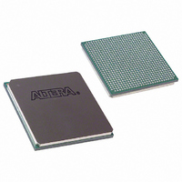
EP3C40F780C6N Altera, EP3C40F780C6N Datasheet - Page 138

EP3C40F780C6N
Manufacturer Part Number
EP3C40F780C6N
Description
IC CYCLONE III FPGA 40K 780FBGA
Manufacturer
Altera
Series
Cyclone® IIIr
Datasheets
1.EP3C5F256C8N.pdf
(5 pages)
2.EP3C5F256C8N.pdf
(34 pages)
3.EP3C5F256C8N.pdf
(66 pages)
4.EP3C5F256C8N.pdf
(14 pages)
5.EP3C5F256C8N.pdf
(76 pages)
6.EP3C40F780C6N.pdf
(274 pages)
Specifications of EP3C40F780C6N
Number Of Logic Elements/cells
39600
Number Of Labs/clbs
2475
Total Ram Bits
1161216
Number Of I /o
535
Voltage - Supply
1.15 V ~ 1.25 V
Mounting Type
Surface Mount
Operating Temperature
0°C ~ 85°C
Package / Case
780-FBGA
Family Name
Cyclone III
Number Of Logic Blocks/elements
39600
# I/os (max)
535
Frequency (max)
500MHz
Process Technology
65nm
Operating Supply Voltage (typ)
1.2V
Logic Cells
39600
Ram Bits
1161216
Operating Supply Voltage (min)
1.15V
Operating Supply Voltage (max)
1.25V
Operating Temp Range
0C to 85C
Operating Temperature Classification
Commercial
Mounting
Surface Mount
Pin Count
780
Package Type
FBGA
For Use With
544-2601 - KIT DEV CYCLONE III LS EP3CLS200544-2411 - KIT DEV NIOS II CYCLONE III ED.
Lead Free Status / RoHS Status
Lead free / RoHS Compliant
Number Of Gates
-
Lead Free Status / Rohs Status
Compliant
Other names
544-2502
Available stocks
Company
Part Number
Manufacturer
Quantity
Price
Part Number:
EP3C40F780C6N
Manufacturer:
ALTERA
Quantity:
20 000
- EP3C5F256C8N PDF datasheet
- EP3C5F256C8N PDF datasheet #2
- EP3C5F256C8N PDF datasheet #3
- EP3C5F256C8N PDF datasheet #4
- EP3C5F256C8N PDF datasheet #5
- EP3C40F780C6N PDF datasheet #6
- Current page: 138 of 274
- Download datasheet (6Mb)
7–14
Figure 7–11. Differential SSTL Class II Interface
Note to
(1) PLL output clock pins do not support differential SSTL-18 Class II I/O standard.
Differential HSTL I/O Standard Support in the Cyclone III Device Family
Figure 7–12. Differential HSTL Class I Interface
Cyclone III Device Handbook, Volume 1
Figure
Output Buffer (1)
7–11:
f
Output Buffer
Figure 7–11
The differential HSTL I/O standard is used for the applications designed to operate in
0 V to 1.2 V, 0 V to 1.5 V, or 0 V to 1.8 V HSTL logic switching range. The Cyclone III
device family supports differential HSTL-18, HSTL-15, and HSTL-12 I/O standards.
The differential HSTL input standard is available on GCLK pins only, treating the
differential inputs as two single-ended HSTL and only decoding one of them. The
differential HSTL output standard is only supported at the PLL#_CLKOUT pins using
two single-ended HSTL output buffers (PLL#_CLKOUTp and PLL#_CLKOUTn), with
the second output programmed to have opposite polarity. The standard requires two
differential inputs with an external reference voltage (VREF), as well as an external
termination voltage (VTT) of 0.5 × V
For more information about the differential HSTL signaling characteristics, refer to the
Cyclone III Device I/O
Data Sheet
Figure 7–12
chapters.
shows the differential SSTL Class II interface.
shows the differential HSTL Class I interface.
V
TT
Features,
Z 0 = 50 Ω
Z 0 = 50 Ω
V
TT
Chapter 7: High-Speed Differential Interfaces in the Cyclone III Device Family
Cyclone III Device Data
V
TT
CCIO
50 Ω
to which termination resistors are connected.
V
TT
V
TT
50 Ω
Sheet, and
V
TT
© December 2009 Altera Corporation
Receiver
High-Speed I/O Standards Support
Cyclone III LS Device
Receiver
Related parts for EP3C40F780C6N
Image
Part Number
Description
Manufacturer
Datasheet
Request
R

Part Number:
Description:
CYCLONE II STARTER KIT EP2C20N
Manufacturer:
Altera
Datasheet:

Part Number:
Description:
CPLD, EP610 Family, ECMOS Process, 300 Gates, 16 Macro Cells, 16 Reg., 16 User I/Os, 5V Supply, 35 Speed Grade, 24DIP
Manufacturer:
Altera Corporation
Datasheet:

Part Number:
Description:
CPLD, EP610 Family, ECMOS Process, 300 Gates, 16 Macro Cells, 16 Reg., 16 User I/Os, 5V Supply, 15 Speed Grade, 24DIP
Manufacturer:
Altera Corporation
Datasheet:

Part Number:
Description:
Manufacturer:
Altera Corporation
Datasheet:

Part Number:
Description:
CPLD, EP610 Family, ECMOS Process, 300 Gates, 16 Macro Cells, 16 Reg., 16 User I/Os, 5V Supply, 30 Speed Grade, 24DIP
Manufacturer:
Altera Corporation
Datasheet:

Part Number:
Description:
High-performance, low-power erasable programmable logic devices with 8 macrocells, 10ns
Manufacturer:
Altera Corporation
Datasheet:

Part Number:
Description:
High-performance, low-power erasable programmable logic devices with 8 macrocells, 7ns
Manufacturer:
Altera Corporation
Datasheet:

Part Number:
Description:
Classic EPLD
Manufacturer:
Altera Corporation
Datasheet:

Part Number:
Description:
High-performance, low-power erasable programmable logic devices with 8 macrocells, 10ns
Manufacturer:
Altera Corporation
Datasheet:

Part Number:
Description:
Manufacturer:
Altera Corporation
Datasheet:

Part Number:
Description:
Manufacturer:
Altera Corporation
Datasheet:

Part Number:
Description:
Manufacturer:
Altera Corporation
Datasheet:

Part Number:
Description:
CPLD, EP610 Family, ECMOS Process, 300 Gates, 16 Macro Cells, 16 Reg., 16 User I/Os, 5V Supply, 25 Speed Grade, 24DIP
Manufacturer:
Altera Corporation
Datasheet:


