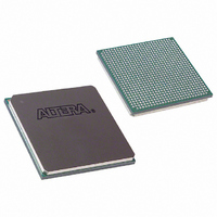
EP3C40F780C6N Altera, EP3C40F780C6N Datasheet - Page 231

EP3C40F780C6N
Manufacturer Part Number
EP3C40F780C6N
Description
IC CYCLONE III FPGA 40K 780FBGA
Manufacturer
Altera
Series
Cyclone® IIIr
Datasheets
1.EP3C5F256C8N.pdf
(5 pages)
2.EP3C5F256C8N.pdf
(34 pages)
3.EP3C5F256C8N.pdf
(66 pages)
4.EP3C5F256C8N.pdf
(14 pages)
5.EP3C5F256C8N.pdf
(76 pages)
6.EP3C40F780C6N.pdf
(274 pages)
Specifications of EP3C40F780C6N
Number Of Logic Elements/cells
39600
Number Of Labs/clbs
2475
Total Ram Bits
1161216
Number Of I /o
535
Voltage - Supply
1.15 V ~ 1.25 V
Mounting Type
Surface Mount
Operating Temperature
0°C ~ 85°C
Package / Case
780-FBGA
Family Name
Cyclone III
Number Of Logic Blocks/elements
39600
# I/os (max)
535
Frequency (max)
500MHz
Process Technology
65nm
Operating Supply Voltage (typ)
1.2V
Logic Cells
39600
Ram Bits
1161216
Operating Supply Voltage (min)
1.15V
Operating Supply Voltage (max)
1.25V
Operating Temp Range
0C to 85C
Operating Temperature Classification
Commercial
Mounting
Surface Mount
Pin Count
780
Package Type
FBGA
For Use With
544-2601 - KIT DEV CYCLONE III LS EP3CLS200544-2411 - KIT DEV NIOS II CYCLONE III ED.
Lead Free Status / RoHS Status
Lead free / RoHS Compliant
Number Of Gates
-
Lead Free Status / Rohs Status
Compliant
Other names
544-2502
Available stocks
Company
Part Number
Manufacturer
Quantity
Price
Part Number:
EP3C40F780C6N
Manufacturer:
ALTERA
Quantity:
20 000
Chapter 9: Configuration, Design Security, and Remote System Upgrades in the Cyclone III Device Family
Configuration Features
Table 9–22. Dedicated Configuration Pins on Cyclone III Device Family (Part 4 of 4)
© December 2009
DATA[7..2]
DATA[15..8]
PADD[23..0]
nRESET
nAVD
nOE
nWE
Note to
(1) AP configuration scheme is for Cyclone III devices only.
Pin Name
Table
9–22:
Altera Corporation
Mode
User
I/O
I/O
I/O
I/O
I/O
I/O
I/O
Configuration
FPP, AP
Scheme
AP
AP
AP
AP
AP
AP
(1)
(1)
(1)
(1)
(1)
(1)
(1)
Bidirectional
Bidirectional
Pin Type
(AP)
Output
Output
Output
Output
Output
Inputs
(FPP).
(1)
Data inputs.
In AS or PS configuration schemes, they function as user I/O
pins during configuration, which means they are tri-stated.
After FPP configuration, DATA[7..2] are available as user
I/O pins and the state of these pin depends on the
Dual-Purpose Pin settings.
The byte-wide or word-wide configuration data is presented
to the target Cyclone III device on
DATA[15..0] , respectively, in the AP configuration
scheme (for Cyclone III devices only). After AP configuration,
DATA[7..2] are dedicated bidirectional pins with optional
user control.
Data inputs. Word-wide configuration data is presented to the
target Cyclone III device on DATA[15..0].
In PS, FPP, or AS configuration schemes, they function as
user I/O pins during configuration, which means they are
tri-stated.
After AP configuration, DATA[15:8] are dedicated
bidirectional pins with optional user control.
24-bit address bus from the Cyclone III device to the parallel
flash in AP mode. Connects to the A[24:1] bus on the
Numonyx P30 or P33 flash.
Active-low reset output. Driving the nRESET pin low resets
the parallel flash. Connects to the RST# pin on the Numonyx
P30 or P33 flash.
Active-low address valid output. Driving the nAVD pin low
during a read or write operation indicates to the parallel flash
that valid address is present on the PADD[23..0] address
bus. Connects to the ADV# pin on the Numonyx P30 or P33
flash.
Active-low output enable to the parallel flash. Driving the
nOE pin low during a read operation enables the parallel flash
outputs (DATA[15..0]). Connects to the OE# pin on the
Numonyx P30 or P33 flash.
Active-low write enable to the parallel flash. Driving the nWE
pin low during a write operation indicates to the parallel flash
that data on the DATA[15..0] bus is valid. Connects to
the WE# pin on the Numonyx P30 or P33 flash.
(1)
Description
Cyclone III Device Handbook, Volume 1
DATA[7..0] or
9–71


