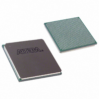
EP3C40F780C6N Altera, EP3C40F780C6N Datasheet - Page 44

EP3C40F780C6N
Manufacturer Part Number
EP3C40F780C6N
Description
IC CYCLONE III FPGA 40K 780FBGA
Manufacturer
Altera
Series
Cyclone® IIIr
Datasheets
1.EP3C5F256C8N.pdf
(5 pages)
2.EP3C5F256C8N.pdf
(34 pages)
3.EP3C5F256C8N.pdf
(66 pages)
4.EP3C5F256C8N.pdf
(14 pages)
5.EP3C5F256C8N.pdf
(76 pages)
6.EP3C40F780C6N.pdf
(274 pages)
Specifications of EP3C40F780C6N
Number Of Logic Elements/cells
39600
Number Of Labs/clbs
2475
Total Ram Bits
1161216
Number Of I /o
535
Voltage - Supply
1.15 V ~ 1.25 V
Mounting Type
Surface Mount
Operating Temperature
0°C ~ 85°C
Package / Case
780-FBGA
Family Name
Cyclone III
Number Of Logic Blocks/elements
39600
# I/os (max)
535
Frequency (max)
500MHz
Process Technology
65nm
Operating Supply Voltage (typ)
1.2V
Logic Cells
39600
Ram Bits
1161216
Operating Supply Voltage (min)
1.15V
Operating Supply Voltage (max)
1.25V
Operating Temp Range
0C to 85C
Operating Temperature Classification
Commercial
Mounting
Surface Mount
Pin Count
780
Package Type
FBGA
For Use With
544-2601 - KIT DEV CYCLONE III LS EP3CLS200544-2411 - KIT DEV NIOS II CYCLONE III ED.
Lead Free Status / RoHS Status
Lead free / RoHS Compliant
Number Of Gates
-
Lead Free Status / Rohs Status
Compliant
Other names
544-2502
Available stocks
Company
Part Number
Manufacturer
Quantity
Price
Part Number:
EP3C40F780C6N
Manufacturer:
ALTERA
Quantity:
20 000
- EP3C5F256C8N PDF datasheet
- EP3C5F256C8N PDF datasheet #2
- EP3C5F256C8N PDF datasheet #3
- EP3C5F256C8N PDF datasheet #4
- EP3C5F256C8N PDF datasheet #5
- EP3C40F780C6N PDF datasheet #6
- Current page: 44 of 274
- Download datasheet (6Mb)
3–8
Memory Modes
Single-Port Mode
Cyclone III Device Handbook, Volume 1
f
1
1
You can selectively enable asynchronous clears per logical memory using the
Quartus II RAM MegaWizard
For more information, refer to the
There are three ways to reset registers in the M9K blocks:
■
■
■
Cyclone III device family M9K memory blocks allow you to implement
fully-synchronous SRAM memory in multiple modes of operation. Cyclone III device
family M9K memory blocks do not support asynchronous (unregistered) memory
inputs.
M9K memory blocks support the following modes:
■
■
■
■
■
■
Violating the setup or hold time on the M9K memory block input registers may
corrupt memory contents. This applies to both read and write operations.
Single-port mode supports non-simultaneous read and write operations from a single
address.
device family M9K memory blocks.
Figure 3–7. Single-Port Memory
Notes to
(1) You can implement two single-port memory blocks in a single M9K block.
(2) For more information, refer to
Power up the device
Use the aclr signal for output register only
Assert the device-wide reset signal using the DEV_CLRn option
Single-port
Simple dual-port
True dual-port
Shift-register
ROM
FIFO
Figure
Figure 3–7
3–7:
shows the single-port memory configuration for Cyclone III
“Packed Mode Support” on page
data[ ]
address[ ]
wren
byteena[]
addressstall
inclocken
rden
aclr
inclock
(Note
™
Plug-In Manager.
RAM Megafunction User
1),
(2)
Chapter 3: Memory Blocks in the Cyclone III Device Family
3–5.
outclocken
outclock
q[]
© December 2009 Altera Corporation
Guide.
Memory Modes
Related parts for EP3C40F780C6N
Image
Part Number
Description
Manufacturer
Datasheet
Request
R

Part Number:
Description:
CYCLONE II STARTER KIT EP2C20N
Manufacturer:
Altera
Datasheet:

Part Number:
Description:
CPLD, EP610 Family, ECMOS Process, 300 Gates, 16 Macro Cells, 16 Reg., 16 User I/Os, 5V Supply, 35 Speed Grade, 24DIP
Manufacturer:
Altera Corporation
Datasheet:

Part Number:
Description:
CPLD, EP610 Family, ECMOS Process, 300 Gates, 16 Macro Cells, 16 Reg., 16 User I/Os, 5V Supply, 15 Speed Grade, 24DIP
Manufacturer:
Altera Corporation
Datasheet:

Part Number:
Description:
Manufacturer:
Altera Corporation
Datasheet:

Part Number:
Description:
CPLD, EP610 Family, ECMOS Process, 300 Gates, 16 Macro Cells, 16 Reg., 16 User I/Os, 5V Supply, 30 Speed Grade, 24DIP
Manufacturer:
Altera Corporation
Datasheet:

Part Number:
Description:
High-performance, low-power erasable programmable logic devices with 8 macrocells, 10ns
Manufacturer:
Altera Corporation
Datasheet:

Part Number:
Description:
High-performance, low-power erasable programmable logic devices with 8 macrocells, 7ns
Manufacturer:
Altera Corporation
Datasheet:

Part Number:
Description:
Classic EPLD
Manufacturer:
Altera Corporation
Datasheet:

Part Number:
Description:
High-performance, low-power erasable programmable logic devices with 8 macrocells, 10ns
Manufacturer:
Altera Corporation
Datasheet:

Part Number:
Description:
Manufacturer:
Altera Corporation
Datasheet:

Part Number:
Description:
Manufacturer:
Altera Corporation
Datasheet:

Part Number:
Description:
Manufacturer:
Altera Corporation
Datasheet:

Part Number:
Description:
CPLD, EP610 Family, ECMOS Process, 300 Gates, 16 Macro Cells, 16 Reg., 16 User I/Os, 5V Supply, 25 Speed Grade, 24DIP
Manufacturer:
Altera Corporation
Datasheet:


