DP83953VUL National Semiconductor, DP83953VUL Datasheet - Page 6
DP83953VUL
Manufacturer Part Number
DP83953VUL
Description
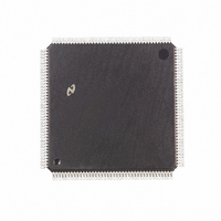
IC CTRLR RIC REPEATER 160-PQFP
Manufacturer
National Semiconductor
Datasheet
1.DP83953VUL.pdf
(90 pages)
Specifications of DP83953VUL
Controller Type
Ethernet Repeater Interface Controller
Interface
IEEE 802.3
Voltage - Supply
4.75 V ~ 5.25 V
Current - Supply
870mA
Operating Temperature
0°C ~ 70°C
Mounting Type
Surface Mount
Package / Case
160-MQFP, 160-PQFP
Lead Free Status / RoHS Status
Contains lead / RoHS non-compliant
Other names
*DP83953VUL
Available stocks
Company
Part Number
Manufacturer
Quantity
Price
Company:

Part Number:
DP83953VUL
Manufacturer:
HJC
Quantity:
2 010
Company:
Part Number:
DP83953VUL
Manufacturer:
Texas Instruments
Quantity:
10 000


2.0 Pin Descriptions
Processor Bus Pins
RA0 - RA4
STR0
STR1
D0 - D7
BUFEN
RDY
ELI
Pin Name
Pin No.
63
66
70
69
68
(Continued)
Driver
Type
TT
TT
C
C
C
C
C
B, Z
I/O
O
O
O
O
O
I
REGISTER ADDRESS INPUTS: These five pins are used to
select a register to be read or written. The state of these inputs
is ignored when the read, write and Mode Load input strobes
are high. (Even under these conditions these inputs must not be
allowed to float at an undefined logic state). See text and table
for proper Mode Load Operation strapping.
DISPLAY UPDATE STROBE 0
Maximum Display Mode: This signal controls the latching of
display data for network ports 1 to 7 into the off chip display
latches.
Minimum Display Mode: This signal controls the latching of
display data for the RIC2A into the off chip display latch.
During processor access cycles (read or write is asserted) this
signal is inactive (high).
DISPLAY UPDATE STROBE 1
Maximum Display Mode: This signal controls the latching of
display data for network ports 8 to 13 into the off chip display
latches.
Minimum Display Mode: No operation
During processor access cycles (read or write is asserted) this
signal is inactive (high).
Data Bus
Display Update Cycles: These pins become outputs providing
display data and port address information.
Processor Access Cycles: Data input or output is performed
via these pins. The read, write and mode load inputs control the
direction of the signals.See text and table for proper Mode Load
Operation strapping.
Note: The data pins remain in their display update function, i.e., asserted as out-
puts unless either the read or write strobe is asserted.
BUFFER ENABLE: This output controls the TRI-STATE
ation of the bus transceiver which provides the interface be-
tween the RIC2A's data pins and the processor's data bus.
Note: The buffer enable output indicates the function of the data pins. When it is
high they are performing display update cycles, when it is low a processor access
or mode load cycle is occurring.
DATA READY STROBE: The falling edge of this signal during
a read cycle indicates that data is stable and valid for sampling.
In write cycles the falling edge of RDY denotes that the write
data has been latched by the RIC2A. Therefore data must have
been available and stable for this operation to be successful.
EVENT LOGGING INTERRUPT: A low level on the ELI output
indicates the RIC2A's hub management logic requires CPU at-
tention. The interrupt is cleared by accessing the Port Event Re-
cording register or Event Counter that produced it. All interrupt
sources may be masked.
6
Description
www.national.com
®
oper-
Related parts for DP83953VUL
Image
Part Number
Description
Manufacturer
Datasheet
Request
R

Part Number:
Description:
Repeater Interface Controller with Security Features, Internal Drivers and Integrated Filters
Manufacturer:
National Semiconductor
Datasheet:
Part Number:
Description:
National Semiconductor [8-Bit D/A Converter]
Manufacturer:
National Semiconductor
Datasheet:
Part Number:
Description:
National Semiconductor [Media Coprocessor]
Manufacturer:
National Semiconductor
Datasheet:
Part Number:
Description:
Digitally Controlled Tone and Volume Circuit with Stereo Audio Power Amplifier, Microphone Preamp Stage and National 3D Sound
Manufacturer:
National Semiconductor
Datasheet:
Part Number:
Description:
Digitally Controlled Tone and Volume Circuit with Stereo Audio Power Amplifier, Microphone Preamp Stage and National 3D Sound
Manufacturer:
National Semiconductor
Datasheet:
Part Number:
Description:
AC97 Rev 2 Codec with Sample Rate Conversion and National 3D Sound
Manufacturer:
National Semiconductor
Part Number:
Description:
Manufacturer:
National Semiconductor
Datasheet:
Part Number:
Description:
Manufacturer:
National Semiconductor
Datasheet:
Part Number:
Description:
General Purpose, Low Voltage, Low Power, Rail-to-Rail Output Operational Amplifiers
Manufacturer:
National Semiconductor
Datasheet:
Part Number:
Description:
8-bit 20 MSPS flash A/D converter.
Manufacturer:
National Semiconductor
Datasheet:
Part Number:
Description:
Low Noise Quad Operational Amplifier
Manufacturer:
National Semiconductor
Datasheet:
Part Number:
Description:
Quad Differential Line Receivers
Manufacturer:
National Semiconductor
Datasheet:
Part Number:
Description:
Quad High Speed Trapezoidal? Bus Transceiver
Manufacturer:
National Semiconductor
Datasheet:
Part Number:
Description:
Dual Line Receiver
Manufacturer:
National Semiconductor
Datasheet: