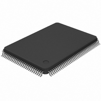
DS21448L+ Maxim Integrated Products, DS21448L+ Datasheet - Page 11

DS21448L+
Manufacturer Part Number
DS21448L+
Description
IC LIU QUAD E1/T1/J1 128-LQFP
Manufacturer
Maxim Integrated Products
Type
Line Interface Units (LIUs)r
Datasheet
1.DS21448L.pdf
(60 pages)
Specifications of DS21448L+
Number Of Drivers/receivers
4/4
Protocol
T1/E1/J1
Voltage - Supply
3.135 V ~ 3.465 V
Mounting Type
Surface Mount
Package / Case
128-TQFP, 128-VQFP
Product
Framer
Number Of Transceivers
4
Supply Voltage (max)
3.465 V
Supply Voltage (min)
3.135 V
Supply Current (max)
400 mA
Maximum Operating Temperature
+ 70 C
Minimum Operating Temperature
0 C
Mounting Style
SMD/SMT
Lead Free Status / RoHS Status
Lead free / RoHS Compliant
Table 2-E. Hardware Interface Mode Pin Description
BPCLK1–BPCLK4
RNEG1–RNEG4
TRING–TRING4
RPOS1–RPOS4
TNEG1–TNEG4
TPOS1–TPOS4
TVDD1–TVDD4
RCLK1–RCLK4
TVSS1–TVSS4
TCLK1–TCLK4
TTIP1–TTIP4
VDD1–VDD4
VSS1–VSS4
L0/L1/L2
JTRST
JTCLK
JAMUX
SCLKE
JTMS
JTDO
VSM
NRZE
JTDI
PIN
HBE
ETS
DJA
JAS
PIN
I/O
—
—
—
—
O
O
O
O
O
O
O
I/O
I
I
I
I
I
I
I
I
I
I
I
I
I
I
I
I
Backplane Clock. A 16.384MHz, 8.192MHz, 4.096MHz, or 2.048MHz clock output that is
referenced to RCLK selectable through CCR5.7 and CCR5.6.
Transmit Tip and Ring. Analog line-driver outputs. These pins connect through a step-up
transformer to the line. See Section
Receive Positive Data. Updated on the rising edge (CCR2.0 = 0) or the falling edge (CCR2.0 = 1)
of RCLK with bipolar data out of the line interface. Set NRZE (CCR1.6) to 1 for NRZ applications.
In NRZ mode, data is output on RPOS, and a received error (BPV, CV, or EXZ) causes a
positive-going pulse synchronous with RCLK at RNEG.
Receive Negative Data. Updated on the rising edge (CCR2.0 = 0) or the falling edge (CCR2.0 =
1) of RCLK with the bipolar data out of the line interface. Set NRZE (CCR1.6) to 1 for NRZ
applications. In NRZ mode, data is output on RPOS, and a received error (BPV, CV, or EXZ)
causes a positive-going pulse synchronous with RCLK at RNEG.
Receive Clock. Buffered recovered clock from the line. Synchronous to MCLK in absence of
signal at RTIP and RRING.
Transmit Positive Data. Sampled on the falling edge (CCR2.1 = 0) or the rising edge (CCR2.1 =
1) of TCLK for data to be transmitted out onto the line.
Transmit Negative Data. Sampled on the falling edge (CCR2.1 = 0) or the rising edge (CCR2.1 =
1) of TCLK for data to be transmitted out onto the line.
Transmit Clock. A 2.048MHz or 1.544MHz primary clock used to clock data through the transmit
side formatter. They can be sourced internally by MCLK or RCLK. See Common Control Register
1 and
JTAG Reset
JTAG Mode Select
JTAG Clock
JTAG Data In
JTAG Data Out
Voltage Supply Mode (LQFP only). VSM should be wired low for correct operation.
3.3V, ±5% Transmitter Positive Supply
3.3V, ±5% Positive Supply
Transmitter Signal Ground for Transmitter Outputs
Signal Ground
E1/T1 Select
0 = E1
1 = T1
NRZ Enable
0 = bipolar data at RPOS/RNEG and TPOS/TNEG
1 = NRZ data at RPOS and TPOS or TNEG; RNEG outputs a positive-going pulse when the
device receives a BPV, CV, or EXZ.
Receive and Transmit Synchronization Clock Enable. SCLKE combines RSCLKE (CCR5.3) and
TSCLKE (CCR5.2).
0 = disable 2.048MHz synchronization transmit and receive mode
1 = enable 2.048MHz synchronization transmit and receive mode
Disable Jitter Attenuator
0 = jitter attenuator enabled
1 = jitter attenuator disabled
Jitter Attenuator Clock Mux. Controls the source for JACLK.
0 = JACLK sourced from MCLK (2.048MHz or 1.544MHz at MCLK).
1 = JACLK sourced from internal PLL (2.048 MHz at MCLK).
Jitter Attenuator Path Select
0 = place the jitter attenuator on the receive side
1 = place the jitter attenuator on the transmit side
Receive and Transmit HDB3/B8ZS Enable. HBE combines RHBE (CCR2.3) and THBE
(CCR2.2).
0 = enable HDB3 (E1)/B8ZS (T1)
1 = disable HDB3 (E1)/B8ZS (T1)
Line Build-Out Select Bits 0,1, and 2. These pins set the transmitter build-out; see
(E1) and
Figure
Table 7-B
1-3.
(T1).
11 of 60
7
for details.
FUNCTION
FUNCTION
(Table 7-A


