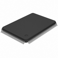
DS21448L+ Maxim Integrated Products, DS21448L+ Datasheet - Page 33

DS21448L+
Manufacturer Part Number
DS21448L+
Description
IC LIU QUAD E1/T1/J1 128-LQFP
Manufacturer
Maxim Integrated Products
Type
Line Interface Units (LIUs)r
Datasheet
1.DS21448L.pdf
(60 pages)
Specifications of DS21448L+
Number Of Drivers/receivers
4/4
Protocol
T1/E1/J1
Voltage - Supply
3.135 V ~ 3.465 V
Mounting Type
Surface Mount
Package / Case
128-TQFP, 128-VQFP
Product
Framer
Number Of Transceivers
4
Supply Voltage (max)
3.465 V
Supply Voltage (min)
3.135 V
Supply Current (max)
400 mA
Maximum Operating Temperature
+ 70 C
Minimum Operating Temperature
0 C
Mounting Style
SMD/SMT
Lead Free Status / RoHS Status
Lead free / RoHS Compliant
7. ANALOG INTERFACE
7.1 Receiver
The DS21448 contains a digital clock recovery system. The DS21448 couples to the receive E1 or T1 twisted pair
(or coaxial cable in 75Ω E1 applications) through a 1:1 transformer. See
Figure
option of using internal termination resistors.
The DS21448 is designed to be fully software selectable for E1 and T1 without the need to change any external
resistors for the receive side. The receive side allows user configuration for 75Ω, 100Ω, or 120Ω receive
termination by setting the RT1 (CCR5.1) and RT0 (CCR5.0) bits. When using the internal termination feature, the
R
be set to 0, and both R
impedance.
The resultant E1 or T1 clock derived from the 2.048/1.544 PLL (JACLK in
through another internal PLL and fed to the clock recovery system. The clock recovery system uses the clock from
the PLL circuit to form a 16-times oversampler used to recover the clock and data. This oversampling technique
offers outstanding performance to meet jitter tolerance specifications, as shown in
Normally, the clock that is output at the RCLK pin is the recovered clock from the E1 AMI/HDB3 or T1 AMI/B8ZS
waveform presented at the RTIP and RRING inputs. When no signal is present at RTIP and RRING, an RCL
condition occurs, and the RCLK is derived from the JACLK source. See
attenuator is placed in the receive path (as is the case in most applications), the jitter attenuator restores the RCLK
to an approximate 50% duty cycle. If the jitter attenuator is either placed in the transmit path or is disabled, the
RCLK output can exhibit slightly shorter high cycles of the clock. This is because of the highly oversampled digital
clock recovery circuitry. See the receive-side AC timing characteristics in Section
The receive-side circuitry also contains a clock synthesizer that outputs a user-configurable clock (up to
16.384MHz) synthesized from RCLK at BPCLK (pin 31). See
BPCLK. In hardware mode, BPCLK defaults to a 16.384MHz output.
The DS21448 has a bypass mode for the receive-side clock and data. This allows the BPCLK to be derived from
RCLK after the jitter attenuator, while the clock and data presented at RCLK, RPOS, and RNEG go unaltered. This
is intended for applications where the receive-side jitter attenuation is done after the LIU. Setting RJAB (CCR6.3) to
logic 1 enables the bypass. Ensure the jitter attenuator is in the receive path (CCR4.3 = 0). See
details.
The DS21448 reports the signal strength at RTIP and RRING in 2.5dB increments through RL3–RL0 located in the
receive information register 2. This feature is helpful when troubleshooting line performance problems
E1 and T1 monitor applications require various flat-gain settings for the receive-side circuitry. The DS21448 can be
programmed to support these applications through the monitor mode control bits MM1 and MM0. When the monitor
modes are enabled, the receiver tolerates normal line loss up to -6dB
7.2 Transmitter
The DS21448 uses a set of laser-trimmed delay lines with a precision digital-to-analog converter (DAC) to create
the waveforms that are transmitted onto the E1 or T1 line. The waveforms meet the latest ETSI, ITU, ANSI, and
AT&T specifications. The user selects which waveform to generate by setting the ETS bit (CCR1.7) for E1 or T1
operation, then programming the L2/L1/L0 bits in common control register 4 for the appropriate application. See
Table 7-A
A 2.048MHz or 1.544MHz TTL clock is required at TCLK for transmitting data at TPOS and TNEG. ITU
specification G.703 requires ±50ppm accuracy for T1 and E1. TR62411 and ANSI specs require ±32ppm accuracy
for T1 interfaces. The clock can be sourced internally by RCLK or JACLK. See CCR1.2, CCR1.1, CCR1.0, and
Figure 1-3
r
resistors should be 60Ω each. See
7-1,
and
Figure
for details. Because of the transmitter’s design, very little jitter (less than 0.005UI
Table 7-B
7-2,
Figure
for the proper L2/L1/L0 settings.
r
resistors
7-3, and
(Figure
Figure 7-1
Table 4-L
7-1) should be 37.5Ω, 50Ω, or 60Ω each, depending on the line
for details. If external termination is required, RT1 and RT0 should
show the receive termination requirements. The DS21448 has the
33 of 60
Table 4-J
(Table
for details about output clock frequencies at
Figure
Figure 1-1
4-K).
Table 7-C
10
Figure
1-1) is internally multiplied by 16
for more details.
for more details. If the jitter
7-7.
for transformer details.
P-P
Figure 1-1
broadband from
(Table
for more
5-B).


