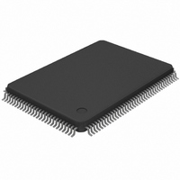
DS21448L+ Maxim Integrated Products, DS21448L+ Datasheet - Page 14

DS21448L+
Manufacturer Part Number
DS21448L+
Description
IC LIU QUAD E1/T1/J1 128-LQFP
Manufacturer
Maxim Integrated Products
Type
Line Interface Units (LIUs)r
Datasheet
1.DS21448L.pdf
(60 pages)
Specifications of DS21448L+
Number Of Drivers/receivers
4/4
Protocol
T1/E1/J1
Voltage - Supply
3.135 V ~ 3.465 V
Mounting Type
Surface Mount
Package / Case
128-TQFP, 128-VQFP
Product
Framer
Number Of Transceivers
4
Supply Voltage (max)
3.465 V
Supply Voltage (min)
3.135 V
Supply Current (max)
400 mA
Maximum Operating Temperature
+ 70 C
Minimum Operating Temperature
0 C
Mounting Style
SMD/SMT
Lead Free Status / RoHS Status
Lead free / RoHS Compliant
4. PORT OPERATION
4.1 Hardware Mode
The DS21448 supports a hardware configuration mode that allows the user to configure the device by setting levels
on the device’s pins. This mode allows the DS21448 configuration without the use of a microprocessor, simplifying
designs. Not all of the device features are supported in the hardware mode.
In hardware mode (BIS0 = 1, BIS1 = 1) several pins have been redefined so they can be used for initializing the
DS21448. Refer to
functions have been combined and affect all four channels in the device and/or treat the receive and transmit paths
as one block. Restrictions when using the hardware mode include the following:
•
•
•
•
•
•
•
•
•
Table 4-A. Loopback Control in Hardware Mode
Table 4-B. Transmit Data Control in Hardware Mode
Table 4-C. Receive Sensitivity Settings in Hardware Mode
Table 4-D. Monitor Gain Settings in Hardware Mode
Table 4-E. Internal Rx Termination Select in Hardware Mode
Remote Loopback
Alternating Ones and Zeros
Analog Loopback
Local Loopback
BPCLK pins only output a 16.384MHz signal.
The RCL/LOTC pins are designated to RCL.
The RHBE and THBE control bits are combined and controlled by HBE.
RSCLKE and TSCLKE bits are combined and controlled by SCLKE.
TCES and RCES are combined and controlled by CES.
The transmitter functions are combined and controlled by TX1 and TX0.
Loopback functions are controlled by LOOP1 and LOOP0.
JABDS defaults to 128-bit buffer depth.
All other control bits default to logic 0.
No Loopback
LOOPBACK
MM1
EGL
RT1
Unframed All Ones
TRANSMIT DATA
0
1
1
0
0
0
1
1
0
0
1
1
TPOS and TNEG
PRBS
0 (E1)
0 (E1)
1 (T1)
1 (T1)
MM0
ETS
RT0
Table 2-B
0
1
0
1
0
1
0
1
SYMBOL
RLB
ALB
LLB
—
INTERNAL LINEAR GAIN BOOST (dB)
and
SYMBOL
TPRBSE
TUA1
TAOZ
Internal receive-side termination disabled
Table 2-E
Normal operation (no boost)
—
TERMINATION CONFIGURATION
Internal receive-side 120Ω enabled
Internal receive-side 100Ω enabled
Internal receive-side 75Ω enabled
LOOP1
RECEIVE SENSITIVITY (dB)
1
1
0
0
-30 (limited long haul)
INTERNAL RECEIVE
-12 (short haul)
-43 (long haul)
-36 (long haul)
for pin assignment and definition. Because of limited pin count, several
20
26
32
TX1
1
1
0
0
LOOP0
14 of 60
1
0
1
0
TX0
1
0
1
0


