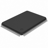
DS21448L+ Maxim Integrated Products, DS21448L+ Datasheet - Page 21

DS21448L+
Manufacturer Part Number
DS21448L+
Description
IC LIU QUAD E1/T1/J1 128-LQFP
Manufacturer
Maxim Integrated Products
Type
Line Interface Units (LIUs)r
Datasheet
1.DS21448L.pdf
(60 pages)
Specifications of DS21448L+
Number Of Drivers/receivers
4/4
Protocol
T1/E1/J1
Voltage - Supply
3.135 V ~ 3.465 V
Mounting Type
Surface Mount
Package / Case
128-TQFP, 128-VQFP
Product
Framer
Number Of Transceivers
4
Supply Voltage (max)
3.465 V
Supply Voltage (min)
3.135 V
Supply Current (max)
400 mA
Maximum Operating Temperature
+ 70 C
Minimum Operating Temperature
0 C
Mounting Style
SMD/SMT
Lead Free Status / RoHS Status
Lead free / RoHS Compliant
CCR3 (02H): Common Control Register 3
CCR4 (03H): Common Control Register 4
TPRBSE
ATUA1
JABDS
NAME
NAME
LIRST
TAOZ
TUA1
TLCE
IBPV
EGL
TPD
DJA
JAS
(MSB)
IBE
(MSB)
TUA1
L2
L1
L0
L2
POSITION
POSITION
CCR3.7
CCR3.6
CCR3.5
CCR3.4
CCR3.3
CCR3.2
CCR3.1
CCR3.0
CCR4.7
CCR4.6
CCR4.5
CCR4.4
CCR4.3
CCR4.2
CCR4.1
CCR4.0
ATUA1
L1
Transmit Unframed All Ones. The polarity of this bit is set such that the device transmits an all-
ones pattern on power-up or device reset. This bit must be set to 1 to allow the device to transmit
data. The transmission of this data pattern is always timed off JACLK
0 = transmit all ones at TTIP and TRING
1 = transmit data normally
Automatic Transmit Unframed All Ones. Automatically transmit an unframed all-ones pattern at
TTIP and TRING during an RCL condition.
0 = disabled
1 = enabled
Transmit Alternate Ones and Zeros. Transmit a …101010… pattern at TTIP and TRING. The
transmission of this data pattern is always timed off TCLK.
0 = disabled
1 = enabled
Transmit PRBS Enable. Transmit a 2
0 = disabled
1 = enabled
Transmit Loop-Code Enable. Enables the transmit side to transmit the loop-up code in the transmit
code definition registers (TCD1 and TCD2). See Section
0 = disabled
1 = enabled
Line Interface Reset. Setting this bit from 0 to 1 initiates an internal reset that resets the clock
recovery state machine and recenters the jitter attenuator. Normally this bit is only toggled on
power-up. It must be cleared and set again for a subsequent reset.
Insert Bipolar Violation (BPV). A 0-to-1 transition on this bit causes a single bipolar violation to be
inserted into the transmit data stream. Once this bit has been toggled from 0 to 1, the device waits
for the next occurrence of three consecutive 1s to insert the BPV. This bit must be cleared and set
again for a subsequent error to be inserted
Insert Bit Error. A 0-to-1 transition on this bit causes a single logic error to be inserted into the
transmit data stream. This bit must be cleared and set again for a subsequent error to be inserted
(Figure
Line Build-Out Select Bit 2. Sets the transmitter build-out
Line Build Out Select Bit 1. Sets the transmitter build-out
Line Build Out Select Bit 0. Sets the transmitter build-out
Receive Equalizer Gain Limit. This bit controls the sensitivity of the receive equalizer
Jitter Attenuator Path Select
0 = place the jitter attenuator on the receive side
1 = place the jitter attenuator on the transmit side
Jitter Attenuator Buffer Depth Select
0 = 128 bits
1 = 32 bits (use for delay-sensitive applications)
Disable Jitter Attenuator
0 = jitter attenuator enabled
1 = jitter attenuator disabled
Transmit Power-Down
0 = normal transmitter operation
1 = powers down the transmitter and tri-states the TTIP and TRING pins
1-3).
TAOZ
L0
TPRBSE
EGL
21 of 60
15
- 1 (E1) or a QRSS (T1) PRBS at TTIP and TRING.
TLCE
JAS
(Figure
FUNCTION
FUNCTION
1-3).
JABDS
LIRST
6
(Table 7-A
(Table 7-A
for details.
(Table 7-A
(Figure
for E1,
for E1,
for E1,
IBPV
DJA
Table 7-B
Table 7-B
Table 7-B
1-1).
(Table
for T1).
for T1).
for T1).
(LSB)
(LSB)
TPD
IBE
4-I).


