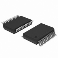
TDA9884TS/V1,112 NXP Semiconductors, TDA9884TS/V1,112 Datasheet - Page 10

TDA9884TS/V1,112
Manufacturer Part Number
TDA9884TS/V1,112
Description
IC IF-PLL I2C-BUS DEMOD 24-SSOP
Manufacturer
NXP Semiconductors
Type
Demodulatorr
Datasheet
1.TDA9884TSV1112.pdf
(58 pages)
Specifications of TDA9884TS/V1,112
Package / Case
*
Applications
Mobile Reception
Mounting Type
Surface Mount
Maximum Operating Temperature
+ 70 C
Minimum Operating Temperature
- 20 C
Mounting Style
SMD/SMT
Lead Free Status / RoHS Status
Lead free / RoHS Compliant
Other names
935270308112
TDA9884TS/V1
TDA9884TS/V1
TDA9884TS/V1
TDA9884TS/V1
Philips Semiconductors
TDA9884_2
Product data sheet
7.7 Video demodulator and amplifier
7.8 Sound carrier trap
7.9 SIF amplifier
The gate time as well as the control logic of the acquisition help circuit is dependent on the
precision of the reference signal at pin REF. Operation as a crystal oscillator is possible as
well as connecting this input via a serial capacitor to an external reference frequency, e.g.
the tuning system oscillator.
The AFC signal is derived from the corresponding down counter stop value after a
counting cycle. The last four bits are latched and can be read out via the I
(see
The video demodulator is realized by a multiplier which is designed for low distortion and
large bandwidth. The VIF signal is multiplied with the ‘in phase’ signal of the VIF-PLL
VCO.
The demodulator output signal is fed into the video preamplifier via a level shift stage with
integrated low-pass filter to achieve carrier harmonics attenuation.
The output signal of the preamplifier is fed to the VIF-AGC detector (see
in the sound trap mode also fed internally to the integrated sound carrier trap
(see
following post-amplifier. The video output level at pin CVBS is 2 V (p-p).
In the bypass mode the output signal of the preamplifier is fed directly through the
post-amplifier to pin CVBS. The output video level is 1.1 V (p-p) for using an external
sound trap with 10 % overall loss.
Noise clipping is provided in both cases.
The sound carrier trap consists of a reference filter, a phase detector and the sound trap
itself.
A sound carrier reference signal is fed into the reference low-pass filter and is shifted by
nominal 90 degrees. The phase detector compares the original reference signal with the
signal shifted by the reference filter and produces a DC voltage by charging or discharging
an integrated capacitor with a current proportional to the phase difference between both
signals, respectively to the frequency error of the integrated filters. The DC voltage
controls the frequency position of the reference filter and the sound trap. So the accurate
frequency position for the different standards is set by the sound carrier reference signal.
The sound trap itself is constructed of three separate traps to realize sufficient
suppression of the first and second sound carriers.
The SIF amplifier consists of three AC-coupled differential stages. Gain control is
performed by emitter degeneration. The total gain control range is typically 66 dB. The
differential input impedance is typically 2 k in parallel with 3 pF.
Table
Section
10). Also the digital-to-analog converted value is given as current at pin AFC.
7.8). The differential trap output signal is converted and amplified by the
Rev. 02 — 12 May 2006
I
2
C-bus controlled multistandard alignment-free IF-PLL
© Koninklijke Philips Electronics N.V. 2006. All rights reserved.
TDA9884
Section
2
C-bus
7.3) and
10 of 58


